Semiconductor nanostructures, semiconductor devices, and methods of making same

a technology of semiconductor devices and nanostructures, applied in the field of semiconductor devices, can solve the problems of incompatibility with requirements, substantial drawbacks, and high cost, and achieve the effect of reducing the cost of semiconductor devices

Inactive Publication Date: 2008-07-17
GLOBALFOUNDRIES INC
View PDF10 Cites 14 Cited by
  • Summary
  • Abstract
  • Description
  • Claims
  • Application Information

AI Technical Summary

Benefits of technology

[0030]forming a field effect transistor (FET) from the semiconductor structure, wherein the FET comprises a source located at one of the two terminal sections of the semiconductor structure, a channel located at the middle section of

Problems solved by technology

This unavoidably results in a transmission probability that is substantially smaller than unity through this interface when an undoped nanowire is used, or in a very substantial shift of the threshold voltage when a uniformly doped nanowire is used for improving the contact quality.
Currently, there are two standard approaches for realizing such a complicated doping profile in a nanowire—both suffering from substantial drawbacks.
This approach, however, is incompatible with the requirement for precisely aligning the FET components, such as the gate and the source/drain metal contacts, at a later

Method used


Image

  • Semiconductor nanostructures, semiconductor devices, and methods of making same
  • Semiconductor nanostructures, semiconductor devices, and methods of making same
  • Semiconductor nanostructures, semiconductor devices, and methods of making same

Examples


Embodiment Construction

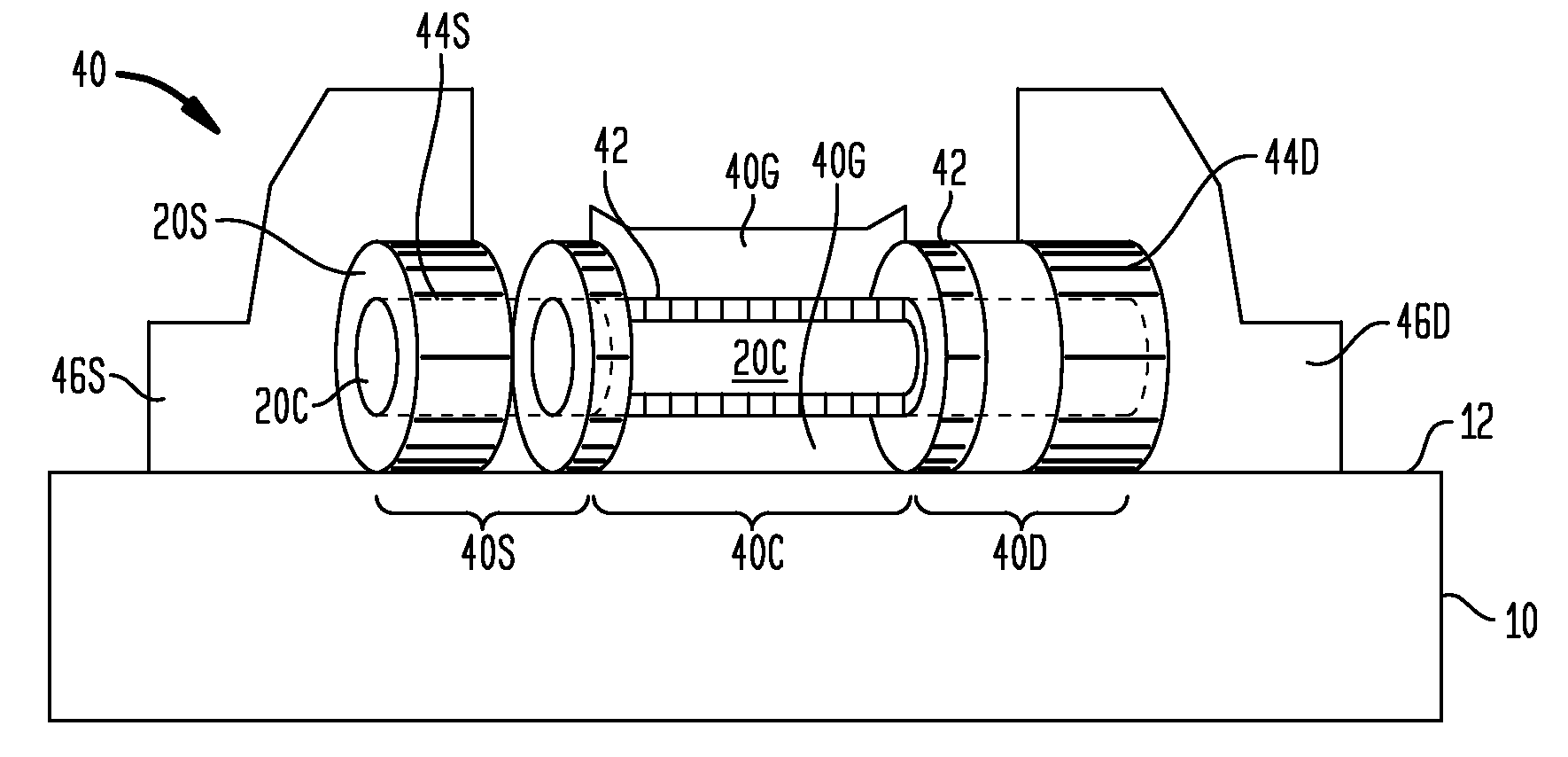
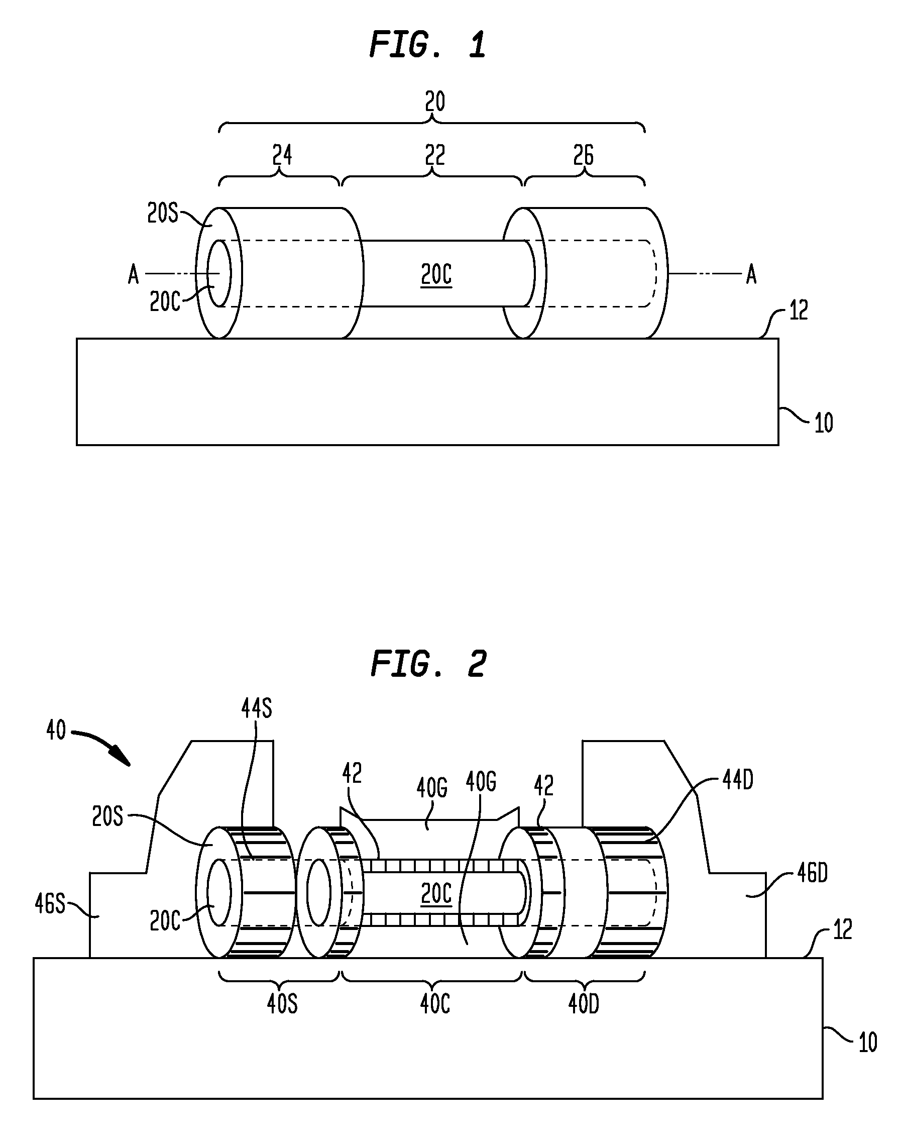
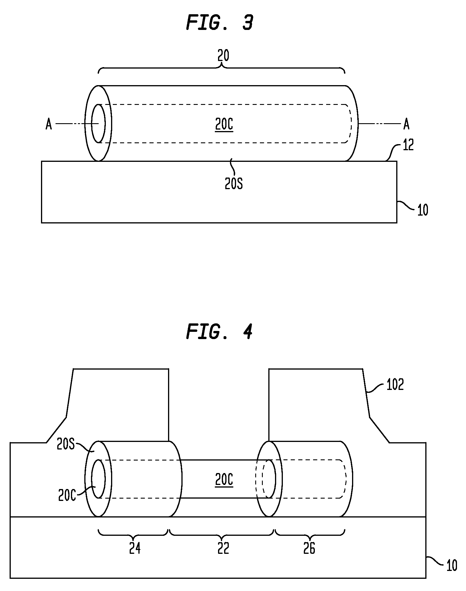
[0038]In the following description, numerous specific details are set forth, such as particular structures, components, materials, dimensions, processing steps and techniques, in order to provide a thorough understanding of the present invention. However, it will be appreciated by one of ordinary skill in the art that the invention may be practiced without these specific details. In other instances, well-known structures or processing steps have not been described in detail in order to avoid obscuring the invention.

[0039]It will be understood that when an element as a layer, region or substrate is referred to as being “on” another element, it can be directly on the other element or intervening elements may also be present. In contrast, when an element is referred to as being “directly on” another element, there are no intervening elements present. It will also be understood that when an element is referred to as being “connected” or “coupled” to another element, it can be directly c...


PUM


Abstract

A semiconductor structure is provided, which includes multiple sections arranged along a longitudinal axis. Preferably, the semiconductor structure comprises a middle section and two terminal sections located at opposite ends of the middle section. A semiconductor core having a first dopant concentration preferably extends along the longitudinal axis through the middle section and the two terminal sections. A semiconductor shell having a second, higher dopant concentration preferably encircles a portion of the terminal sections, but not at the middle section, of the semiconductor structure. It is particularly preferred that the semiconductor structure is a nanostructure having a cross-sectional dimension of not more than 100 nm.

Description

[0001]This invention was made with Government support under Contract No. 66001-05-C-8043 awarded by the Defense Advanced Research Project Agency (DARPA). The Government thus has certain rights to this invention.FIELD OF THE INVENTION[0002]The present invention generally relates to semiconductor nanostructures with a core-shell configuration that can be used for forming nano-sized semiconductor devices. More specifically, the present invention relates to field effect transistors (FETs) formed by such semiconductor nanostructures, as well as to methods for forming the FETs.BACKGROUND OF THE INVENTION[0003]Miniaturization of semiconductor devices, such as field effect transistors (FETs), has been the main driving force behind the incredible progress in the area of computation over the last half decade. Use of smaller FETs advantageously results in a higher packing density, as well as improved device performance. To further sustain this trend, novel nanostructures are explored as possib...

Claims


Application Information

Patent Timeline
IPC IPC(8): H01L29/78H01L21/04
CPCB82Y10/00H01L29/0665H01L29/0673H01L29/068H01L29/125H01L21/30604H01L29/78696H01L29/1041H01L29/66439H01L21/02603H01L29/42392B82B1/00B82B3/00B82Y40/00
Inventor APPENZELLER, JOERGGUHA, SUPRATIKTUTUC, EMANUEL
Owner GLOBALFOUNDRIES INC
Why Eureka
Try Eureka