Driving circuit of driving light-emitting device
- Summary
- Abstract
- Description
- Claims
- Application Information
AI Technical Summary
Benefits of technology
Problems solved by technology
Method used
Image
Examples
first embodiment
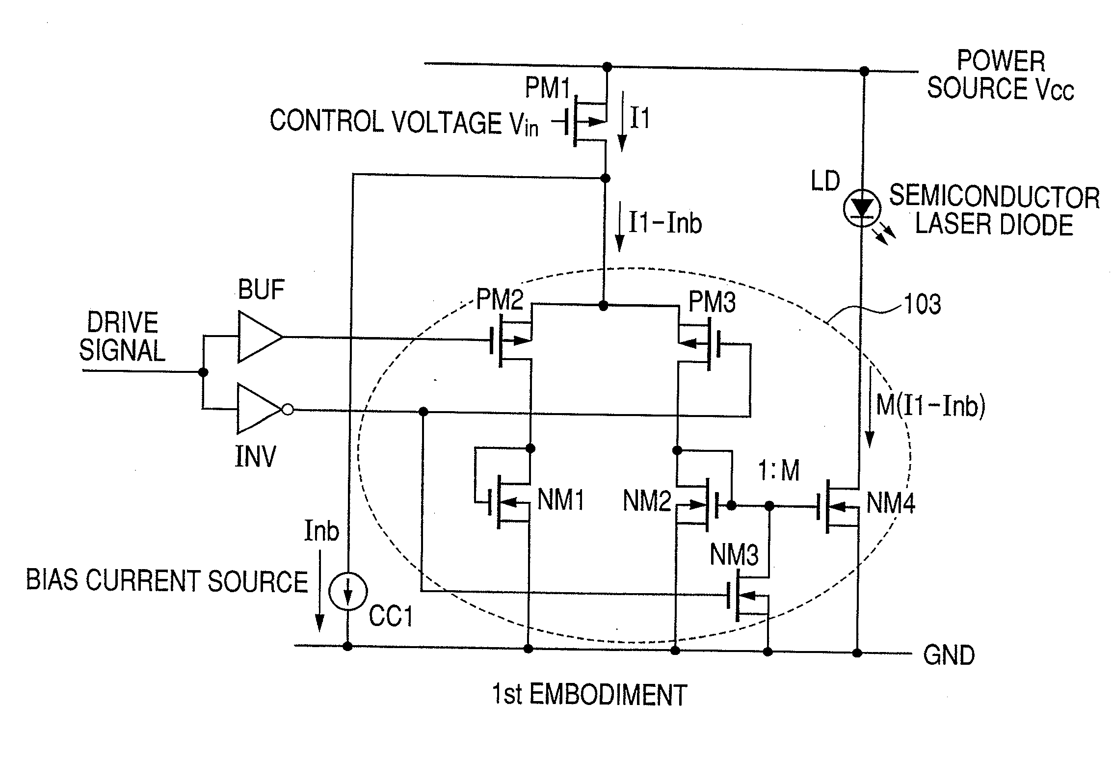
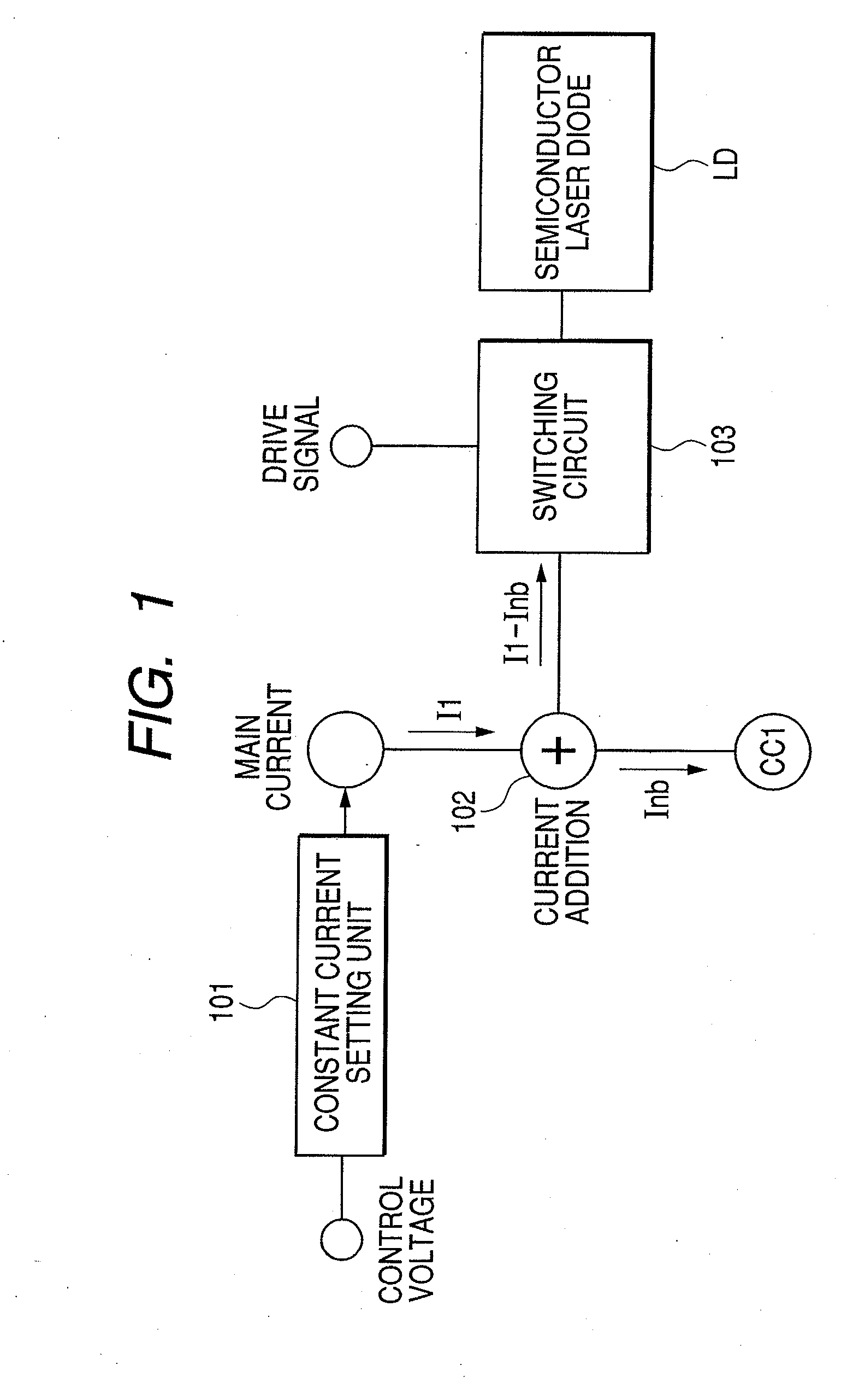
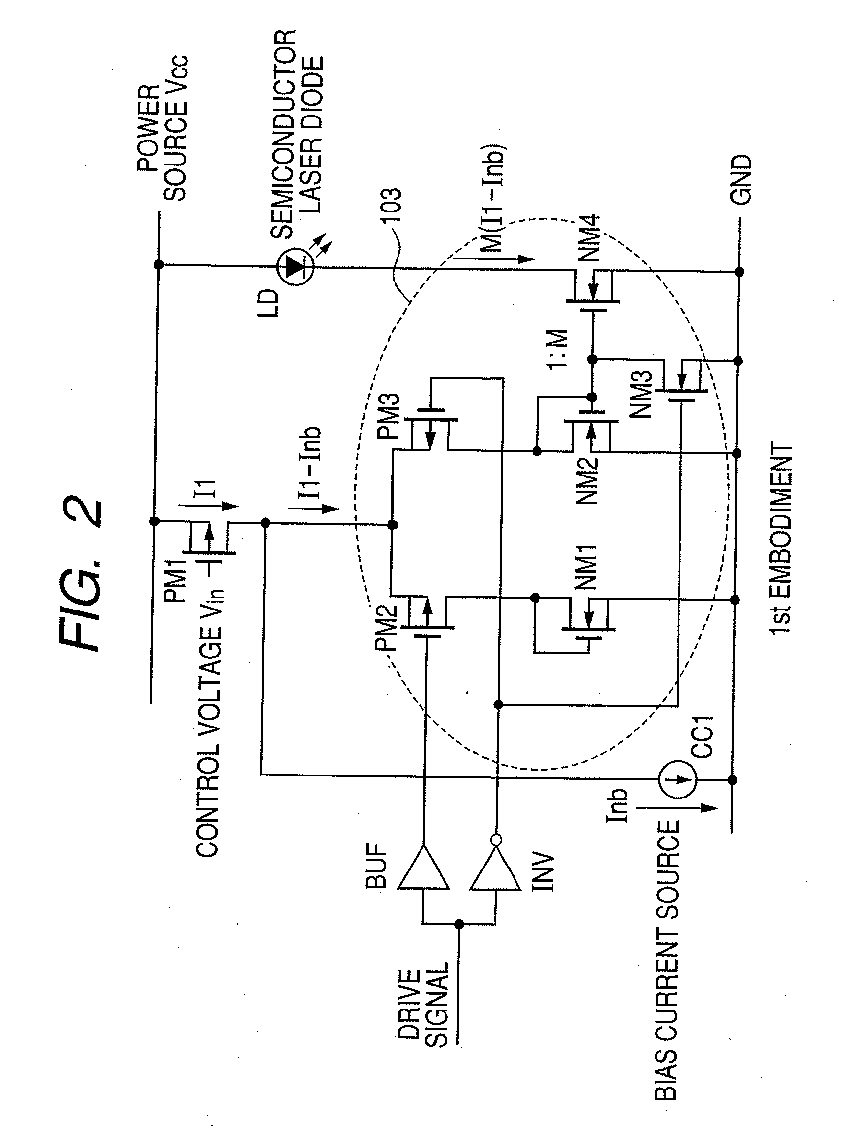
[0018]FIG. 1 is a diagram showing an example of a conceptual configuration of a semiconductor laser diode drive circuit (a driving circuit of driving a light-emitting device) according to a first exemplary embodiment of the present invention. Description will be made an example of a case where a semiconductor laser diode is used as a light-emitting device.
[0019]A control voltage is input to a current control unit 101. The current control unit (also referred to as a constant current setting unit below) 101 controls the value of a main current I1 for setting a drive current for driving a semiconductor laser diode LD. The main current II is a constant current. A bias current source CC1 is a bias current source for subtracting a bias current Inb from the main current I1.
[0020]The current obtained by subtracting the bias current Inb from the main current I1 is I1−Inb. A current addition unit 102 adds together the main current I1 and the negative bias current Inb and outputs the current I...
second embodiment
[0032]FIG. 3 is a circuit diagram showing an example of a configuration of a semiconductor laser diode drive circuit according to a second exemplary embodiment of the present invention. In the second exemplary embodiment, a gate-grounded PMOS transistor PM4 is inserted between the transistor PM1 and the transistors PM2 and PM3 in the configuration of the first embodiment shown in FIG. 2. In other respects, the second exemplary embodiment is the same as the first exemplary embodiment. A bias voltage Vbias enough for securing the desired source-drain voltage of the transistors PM2 and PM3 is applied to the gate of the transistor PM4. The transistor PM4 is connected between the switching unit 103 and the connection node between the transistor PM1 (constant current setting unit 101) and the bias current source CC1 as a load for constantly maintaining the node potential with respect to the sum current I1−Inb. Thus, a characteristic free from the Early effect of the transistor PM1 on the ...
third embodiment
[0033]FIG. 4 is a circuit diagram showing an example of a configuration of a semiconductor laser diode drive circuit according to a third exemplary embodiment of the present invention. The third exemplary embodiment represents an application of the present invention to a differential-type drive current switching system.
[0034]A PNP bipolar transistor BP1 has its emitter connected to a power supply voltage Vcc. A main current I1 flows through the collector of the PNP bipolar transistor BP1. An NPN bipolar transistor BN1 has its collector connected to the collector of the transistor BP1 and has its emitter grounded. The gate and the collector of the transistor BN1 are connected to each other. A bias current source CC1 is connected between the collector of the transistor BN1 and ground to draw in a constant current Inb. An NPN bipolar transistor BN2 has its base connected to the base of the transistor BN1 and has its emitter grounded. The size of the transistor BN2 is an M multiple of t...
PUM
 Abstract
Description
Claims
Application Information


