Driving circuit of driving light-emitting device

a technology of driving circuit and light-emitting device, which is applied in the direction of pulse technique, semiconductor laser, instruments, etc., can solve the problem of large drive current, and achieve the effect of reliable emission control

Inactive Publication Date: 2011-03-08
CANON KK
View PDF8 Cites 1 Cited by
  • Summary
  • Abstract
  • Description
  • Claims
  • Application Information

AI Technical Summary

Benefits of technology

[0008]An object of the present invention is to provide a light limiting device driving circuit capable of reliably performing emission control on a light-emitting device of a low emission threshold (about 10 mA or less) and capable of correcting a distortion due to the Early effect of a transistor in the drive current supplied to the light emitting device.
[0010]The present invention enables a light-emitting device of a low emission threshold to be controlled with reliability. The present invention also enables correction of a distortion due to the Early effect of a transistor in the drive current supplied to the light-emitting device.

Problems solved by technology

Accordingly, it is likely that, even at a minimum control voltage, an excessive drive current larger than a suitable level for a desired light emission quantity would flow thereto.

Method used


Image

  • Driving circuit of driving light-emitting device
  • Driving circuit of driving light-emitting device
  • Driving circuit of driving light-emitting device

Examples


first embodiment

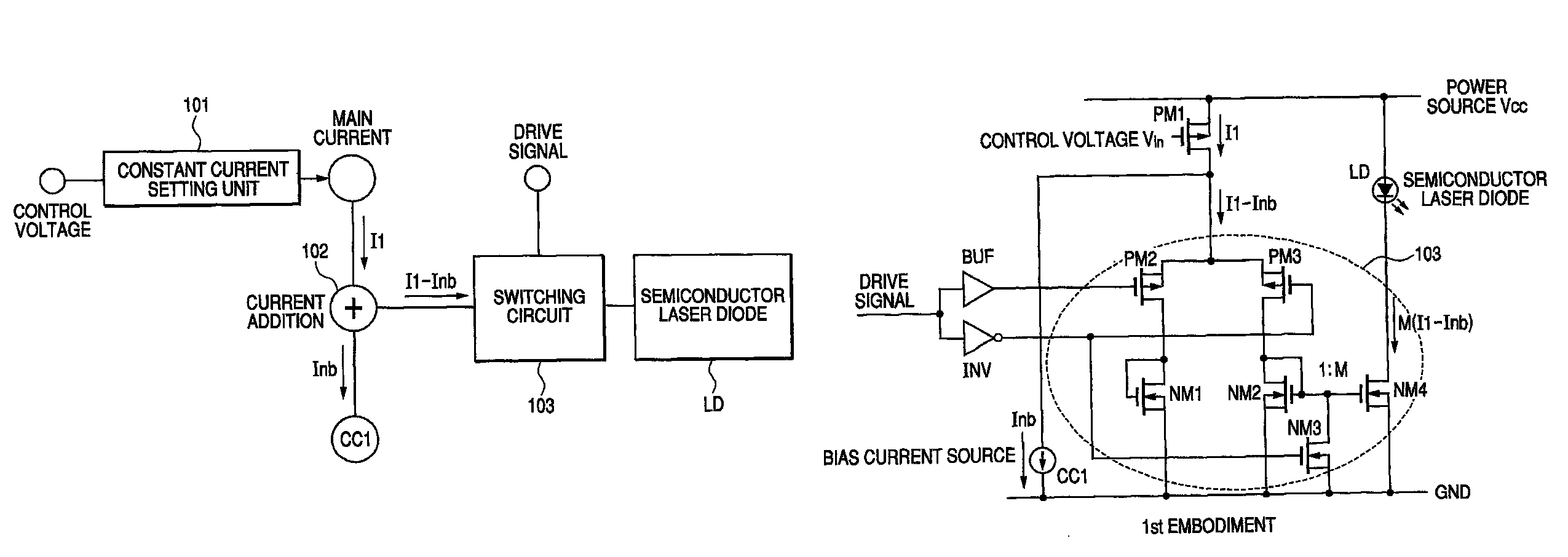
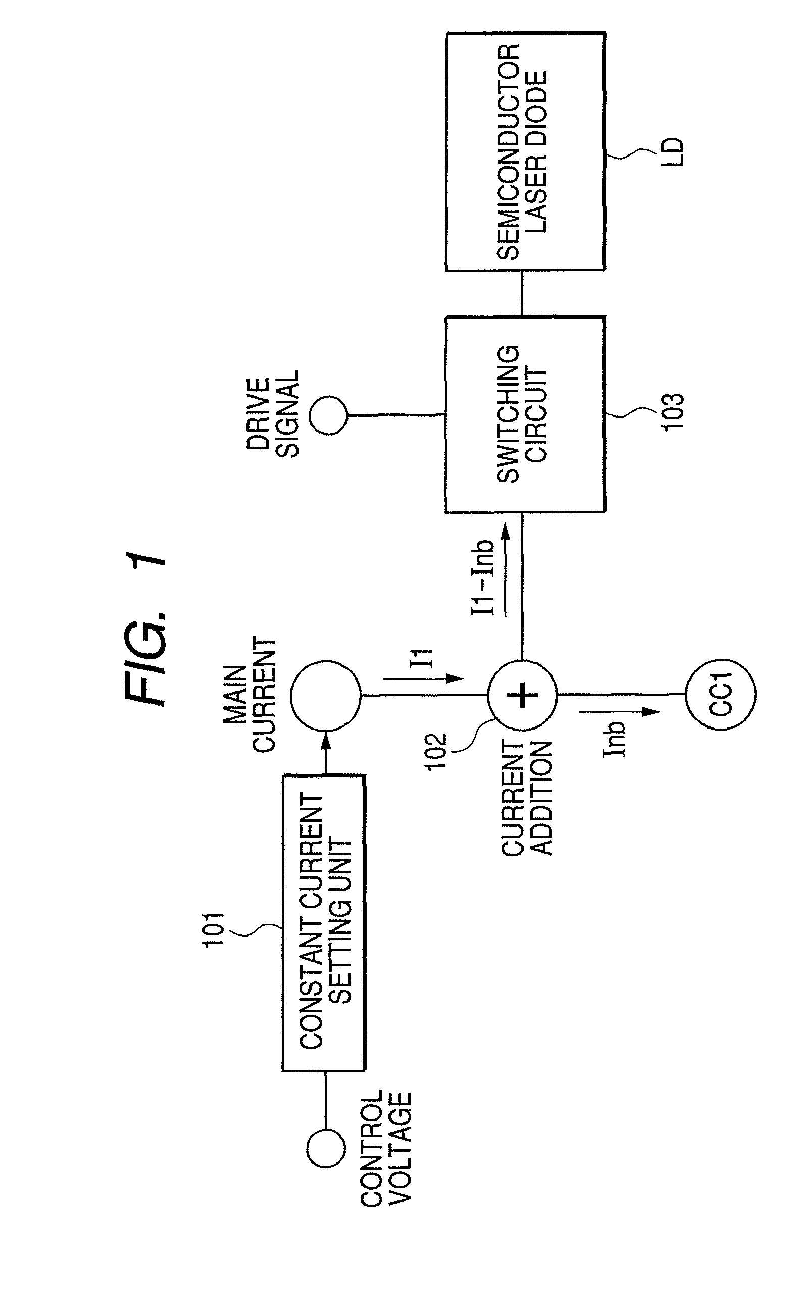
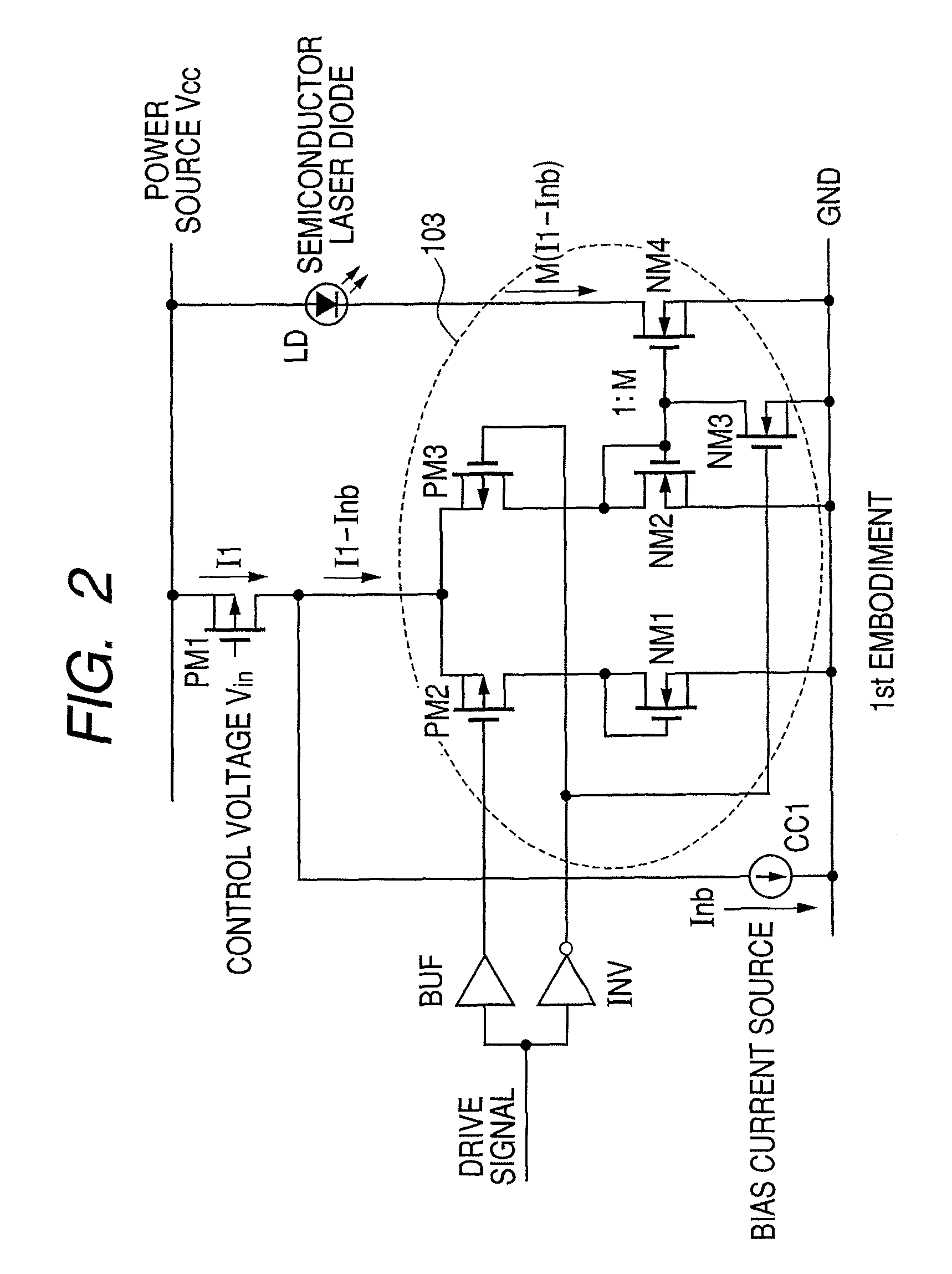
[0018]FIG. 1 is a diagram showing an example of a conceptual configuration of a semiconductor laser diode drive circuit (a driving circuit of driving a light-emitting device) according to a first exemplary embodiment of the present invention. Description will be made an example of a case where a semiconductor laser diode is used as a light-emitting device.

[0019]A control voltage is input to a current control unit 101. The current control unit (also referred to as a constant current setting unit below) 101 controls the value of a main current I1 for setting a drive current for driving a semiconductor laser diode LD. The main current I1 is a constant current. A bias current source CC1 is a bias current source for subtracting a bias current Inb from the main current I1. The current obtained by subtracting the bias current Inb from the main current I1 is I1−Inb. A current addition unit 102 adds together the main current I1 and the negative bias current Inb and outputs the current I1−Inb...

second embodiment

[0030]FIG. 3 is a circuit diagram showing an example of a configuration of a semiconductor laser diode drive circuit according to a second exemplary embodiment of the present invention. In the second exemplary embodiment, a gate-grounded PMOS transistor PM4 is inserted between the transistor PM1 and the transistors PM2 and PM3 in the configuration of the first embodiment shown in FIG. 2. In other respects, the second exemplary embodiment is the same as the first exemplary embodiment. A bias voltage Vbias enough for securing the desired source-drain voltage of the transistors PM2 and PM3 is applied to the gate of the transistor PM4. The transistor PM4 is connected between the switching unit 103 and the connection node between the transistor PM1 (constant current setting unit 101) and the bias current source CC1 as a load for constantly maintaining the node potential with respect to the sum current I1−Inb. Thus, a characteristic free from the Early effect of the transistor PM1 on the ...

third embodiment

[0031]FIG. 4 is a circuit diagram showing an example of a configuration of a semiconductor laser diode drive circuit according to a third exemplary embodiment of the present invention. The third exemplary embodiment represents an application of the present invention to a differential-type drive current switching system.

[0032]A PNP bipolar transistor BP1 has its emitter connected to a power supply voltage Vcc. A main current I1 flows through the collector of the PNP bipolar transistor BP1. An NPN bipolar transistor BN1 has its collector connected to the collector of the transistor BP1 and has its emitter grounded. The gate and the collector of the transistor BN1 are connected to each other. A bias current source CC1 is connected between the collector of the transistor BN1 and ground to draw in a constant current Inb. An NPN bipolar transistor BN2 has its base connected to the base of the transistor BN1 and has its emitter grounded. The size of the transistor BN2 is an M multiple of t...


PUM


Abstract

A light-emitting device driving circuit capable of reliably performing emission control on a light-emitting device of a low emission threshold (about 10 mA or less) and capable of correcting a distortion due to the Early effect of a transistor in the drive current supplied to the light emitting device. The light limiting device driving circuit includes a current control unit (101) which controls the value of a main current based on a control voltage, a bias current source (CC1) for subtracting a bias current from the main current, and a switching unit (103) which controls emission of light from the light-emitting device by switching, based on the drive signal, a current obtained by subtracting the bias current from the main current or a current based on the current obtained by the subtraction.

Description

BACKGROUND OF THE INVENTION[0001]1. Field of the Invention[0002]The present invention relates to a driving circuit of driving a light-emitting device.[0003]2. Description of the Related Art[0004]Semiconductor laser diodes are being widely used, for example, for writing in laser beam printers (LBPs) and for writing to or reading from various recording mediums such as compact disks (CDs) and digital versatile disks (DVDs) because they are small in size and low in power consumption. A semiconductor laser diode emits light when a certain threshold current is exceeded. In recent years, with the remarkable reduction in threshold value and improvement in emission efficiency, it has been possible to obtain by a drive current of several milliamperes the amount of emission of light for which a drive current of several ten milliamperes is required in the conventional semiconductor laser diodes. In LBPs, the number of output sheets per minute depends on the switching speed of a semiconductor la...

Claims


Application Information

Patent Timeline
Patent Type & Authority Patents(United States)
IPC IPC(8): G05F1/10
CPCH01S5/042H01S5/0427
Inventor NAKAMURA, HIROYUKI
Owner CANON KK
Why Eureka
Try Eureka