Pinned photodiode CMOS image sensor with a low supply voltage

a photosensitive cell, monolithic technology, applied in the direction of instruments, television systems, television system scanning details, etc., can solve the problems of affecting the operation of the image sensor. , to achieve the effect of reducing the voltage vsub>rt /sub>, reducing the voltage vsub>rst /sub>, and reducing the voltage vsub>

Active Publication Date: 2008-07-17
STMICROELECTRONICS SRL
View PDF6 Cites 17 Cited by
  • Summary
  • Abstract
  • Description
  • Claims
  • Application Information

AI Technical Summary

Benefits of technology

[0016]In an embodiment, the present invention aims at a pinned photodiode image sensor with a decreased power supply providing an appropriate charge transfer from the photodiode to the sense node while keeping proper linearity properties.

Problems solved by technology

However, several difficulties arise when supply voltage VRT is decreased.
A first difficulty is that the decrease of voltage VRT translates as a decrease in voltage VRST.
With the previously-described image sensor controlling method, it can then be difficult, or even impossible, to adjust voltages VD and VT to ensure the proper transfer of the charges of photodiode D to sense node SN while keeping an appropriate swing of voltage VSN and an appropriate swing of the photodiode voltage.
Another difficulty is to ensure for transistor M2 to operate in linear state across the entire swing of voltage VSN to ensure for the voltage at node X to be a linear reproduction of voltage VSN.
With the previously-described image control method, it may be difficult, or even impossible, when VRT is desired to be decreased, to have the range of voltage VSN for which transistor M2 is in linear state correspond to the range of voltage VSN for which a proper charge transfer from photodiode D to sense node SN is obtained.

Method used


Image

  • Pinned photodiode CMOS image sensor with a low supply voltage
  • Pinned photodiode CMOS image sensor with a low supply voltage
  • Pinned photodiode CMOS image sensor with a low supply voltage

Examples


Embodiment Construction

[0041]For clarity, the same elements have been designated with the same reference numerals in the different drawings and, further, as usual in the representation of integrated circuits, the various drawings are not to scale.

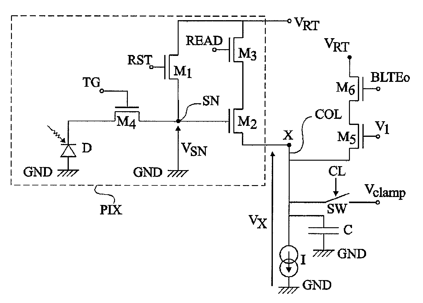
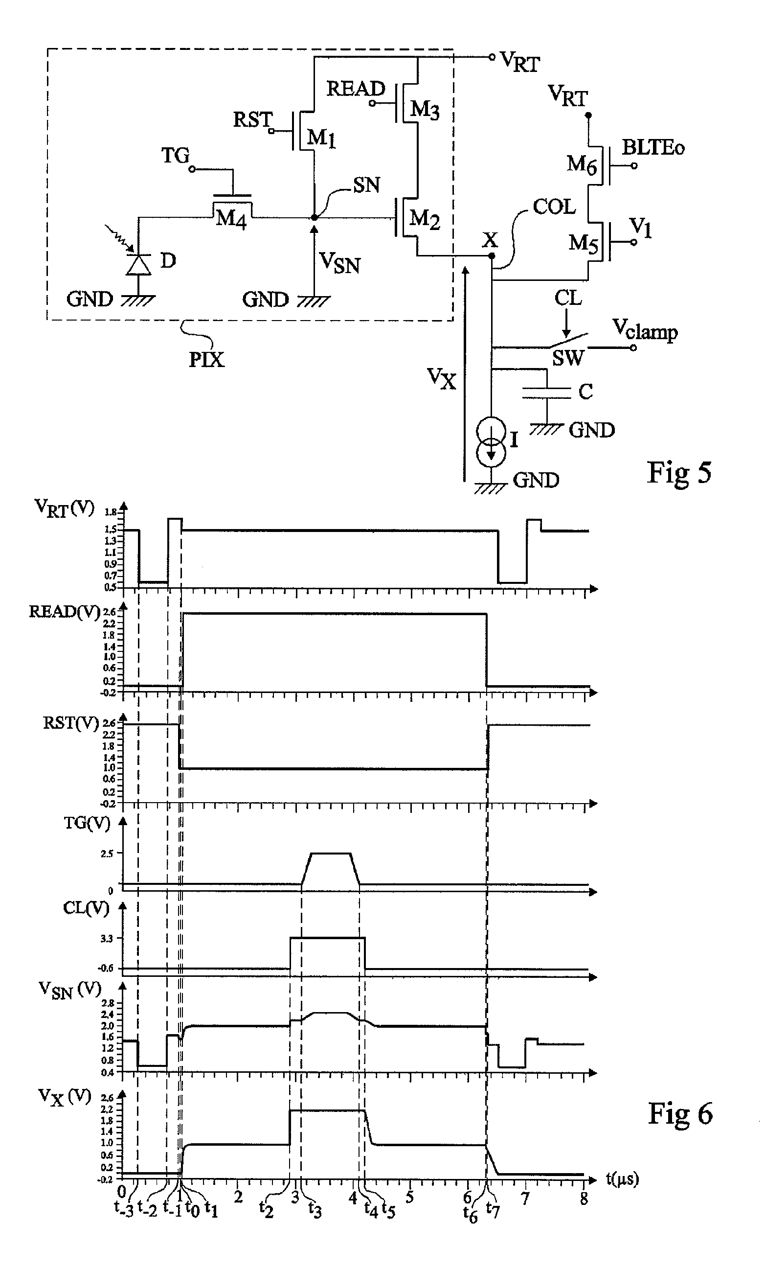
[0042]In an embodiment, the present invention comprises separating the charge transfer problem from the problem of the linear operation of transistor M2 on reading of the signal from the sense node. For this purpose, the fact that, just after the charge transfer to the sense node, the sense node is at a floating potential, is used. An embodiment of the present invention then comprises temporarily increasing voltage VSN during the charge transfer phase by capacitive coupling effect, to ease the transfer of charges from the photodiode to the sense node. Further, the circuit parameters are adjusted to ensure that, during a read cycle, outside of the charge transfer phase, transistor M2 is in linear state. In order to obtain an efficient capacitive coupling effect, i...


PUM


Abstract

A device for controlling an image sensor including at least one photosensitive cell including a photodiode capable of discharging into a sense node via a first MOS transistor, the sense node being connected to the gate of a second MOS transistor having its source connected to a processing system. The device includes a bias circuit capable of increasing the voltage of the source during the discharge of the photodiode into the sense node.

Description

BACKGROUND OF THE INVENTION[0001]1. Field of the Invention[0002]The present invention relates to the control of a monolithic photosensitive cell of an image sensor for use in image shooting devices such as, for example, film cameras, camcorders, digital photographic devices, or again cellular phones. More specifically, the present invention relates to a semiconductor-based photosensitive cell.[0003]2. Discussion of the Related Art[0004]FIG. 1 schematically illustrates the circuit of a photosensitive cell PIX, or pixel, of an array of photosensitive cells of an image sensor. With each photosensitive cell of the array are associated a precharge device and a read device. The precharge device is formed of an N-channel MOS transistor M1, interposed between a supply rail VRT and a sense node SN. The gate of precharge transistor M1 is capable of receiving a precharge control signal RST. The read device is formed of the series connection of first and second N-channel MOS transistors M3, M2....

Claims


Application Information

Patent Timeline
Patent Type & Authority Applications(United States)
IPC IPC(8): H04N3/14H04N5/359H04N5/3745
CPCH04N5/3745H04N5/3597H04N25/626H04N25/77
Inventor BARBIER, FREDERICCAZAUX, YVON
Owner STMICROELECTRONICS SRL
Why Eureka
Try Eureka