Wafer-scale image archiving and receiving system

Inactive Publication Date: 2008-07-17
NANOARK CORP
View PDF9 Cites 9 Cited by
  • Summary
  • Abstract
  • Description
  • Claims
  • Application Information

AI Technical Summary

Benefits of technology

[0012]An advantage of the present invention is that large amounts of stored data are compactly stored and can be accessed very rapidly.
[0013]A further advantage of the present invention is that the ima

Problems solved by technology

Due to the sheer volume of the above described data, paper-based storage is expensive and very cumbersome.
Furthermore, paper is susceptible to environmental hazards such as water and fire.
Paper documents do not age well with time unless great care is taken to preserve the paper.
However, this technology requires special microfilm viewers to view the images.
Furthermore, high-quality hard-copy reproduction is expensive and

Method used


Image

  • Wafer-scale image archiving and receiving system
  • Wafer-scale image archiving and receiving system
  • Wafer-scale image archiving and receiving system

Examples


Example

[0020]Corresponding reference characters indicate corresponding parts throughout the several views. The examples set out herein illustrate several embodiments of the invention but should not be construed as limiting the scope of the invention in any manner.

DETAILED DESCRIPTION

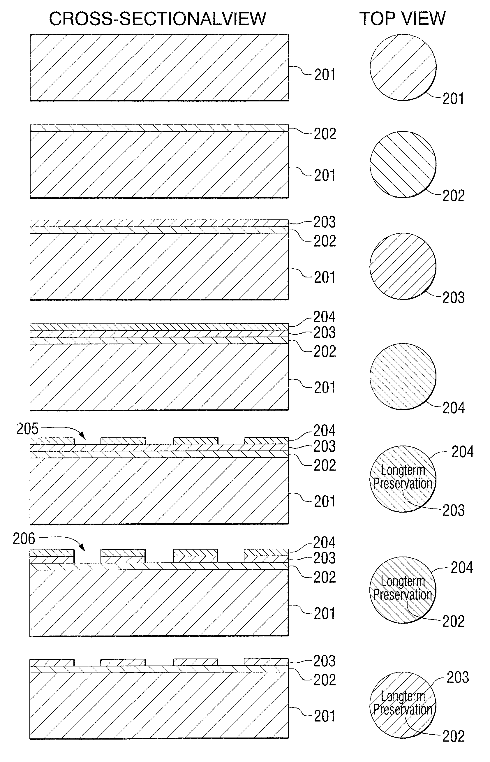
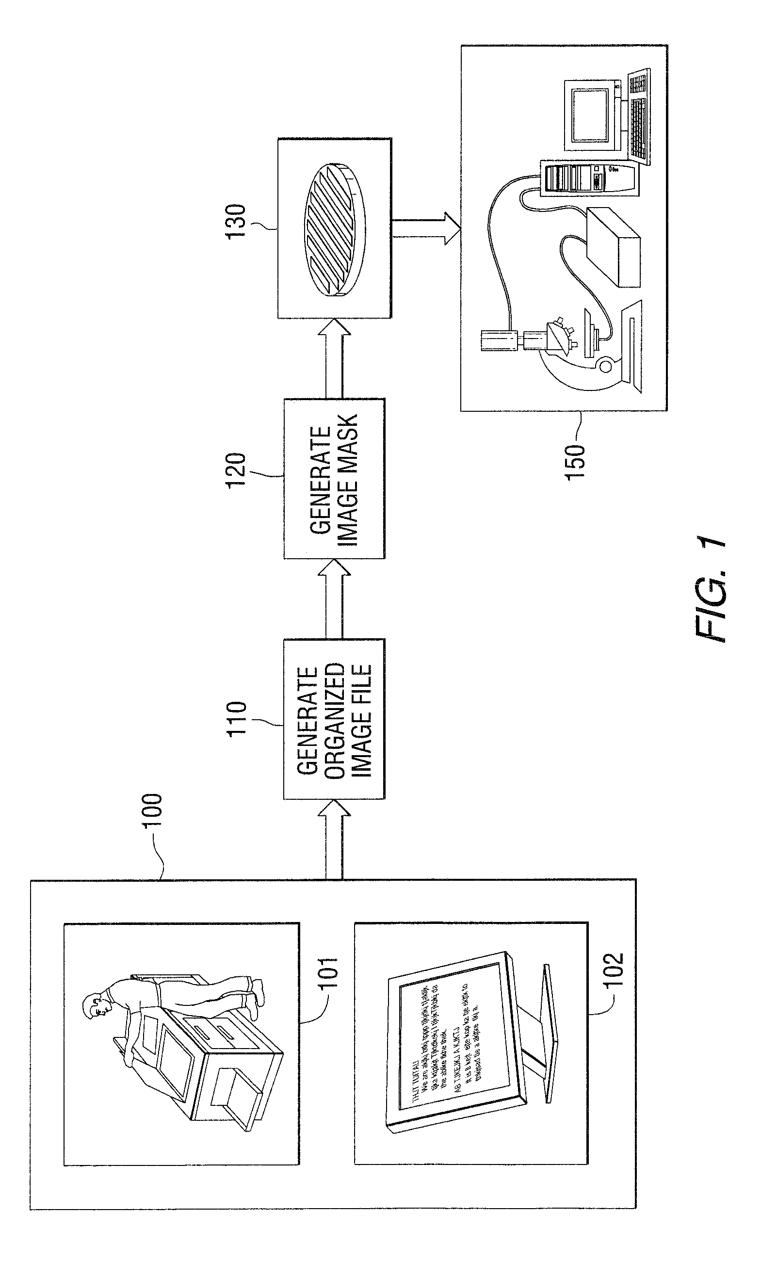
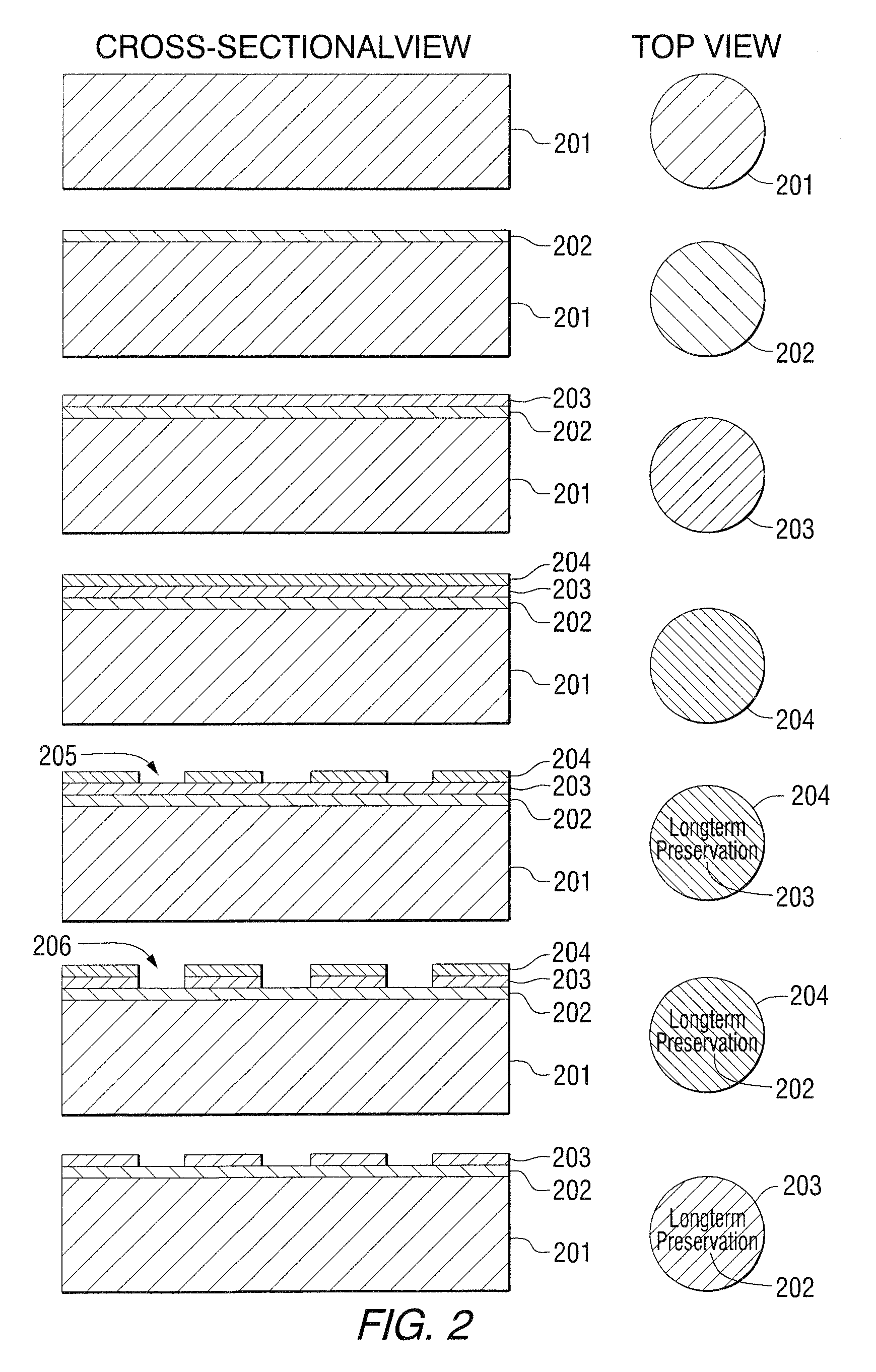
[0021]This invention relates to storing data as images on semiconductor substrates, particularly for long-term preservation using imaging and semiconductor fabrication techniques. In this technique, data are stored in such a way that it is visible to the human eye usually with magnification, though it is possible to view large-scale images without magnification. The data from printed documents, digital files, or any other media are converted to images. These images, with the help of photolithography tools and fabrication techniques, are then imprinted and etched on semiconductor substrates, such as silicon wafers. The use of silicon makes the information resistant to both high temperatures up to 400° C. and wat...


PUM


Abstract

A system for the long-term storage and high-speed retrieval of images stored on silicon wafers. The images are stored by utilizing semiconductor fabrication techniques. These images are organized and managed using metadata in the form of a barcode. Each barcode is a unique identifier that contains the location information for each specific image on the silicon wafer substrate. The system further provides an identifier in an electronic database that references the appropriate barcode and describes the contents of the image. The images and barcodes are transferred to specific predetermined locations on the silicon wafer. The stored images are retrieved by use of a software program that searches for a user's queries in the electronic database and outputs the specific barcode to the image reader. The image reader translates the barcode information for the desired image and drives the optics or the silicon wafer to the appropriate location.

Description

CROSS-REFERENCE TO RELATED APPLICATIONS[0001]This application claims priority from U.S. Provisional Patent Application Ser. No. 60 / 884,768, titled PRESERVATION / STORAGE OF DATA AS IMAGES ON SILICON WAFERS USING NANOTECHNOLOGY, filed Jan. 12, 2007, which is hereby incorporated by reference.FIELD OF THE INVENTION[0002]This invention relates to the long-term storage of images on substrates that can be processed using semiconductor fabrication techniques, and more particularly to the long-term storage of images on silicon wafer substrates. The invention further relates to the high-speed retrieval of images stored on silicon wafer substrates.BACKGROUND OF THE INVENTION[0003]As unique documents are created and the desire to back-up information is increased the need effectively to archive data increases. On an individual level, information such as letters, property papers, financial documents, photographs and such are preserved for sentimental, personal, and financial reasons. Federal insti...

Claims


Application Information

Patent Timeline
IPC IPC(8): G06K9/00
CPCG06F17/30011G06F16/93
Inventor PASUPULETI, AJAY
Owner NANOARK CORP
Why Eureka
Try Eureka