
Heterojunction bipolar transistor having (In) (Al) GaAsSb/InGaAs base-collector structure
a bipolar transistor and base-collector technology, applied in the direction of basic electric elements, electrical apparatus, semiconductor devices, etc., can solve the problems of difficult to achieve high current density, difficult to obtain high current density, and hinder the electrons, so as to achieve effective infusing electrons, improve electron transference, and high drift velocity
- Summary
- Abstract
- Description
- Claims
- Application Information
AI Technical Summary
Benefits of technology
Problems solved by technology
Method used
Image

Examples
Embodiment Construction
[0024]The following descriptions of the preferred embodiments are provided to understand the features and the structures of the present invention.
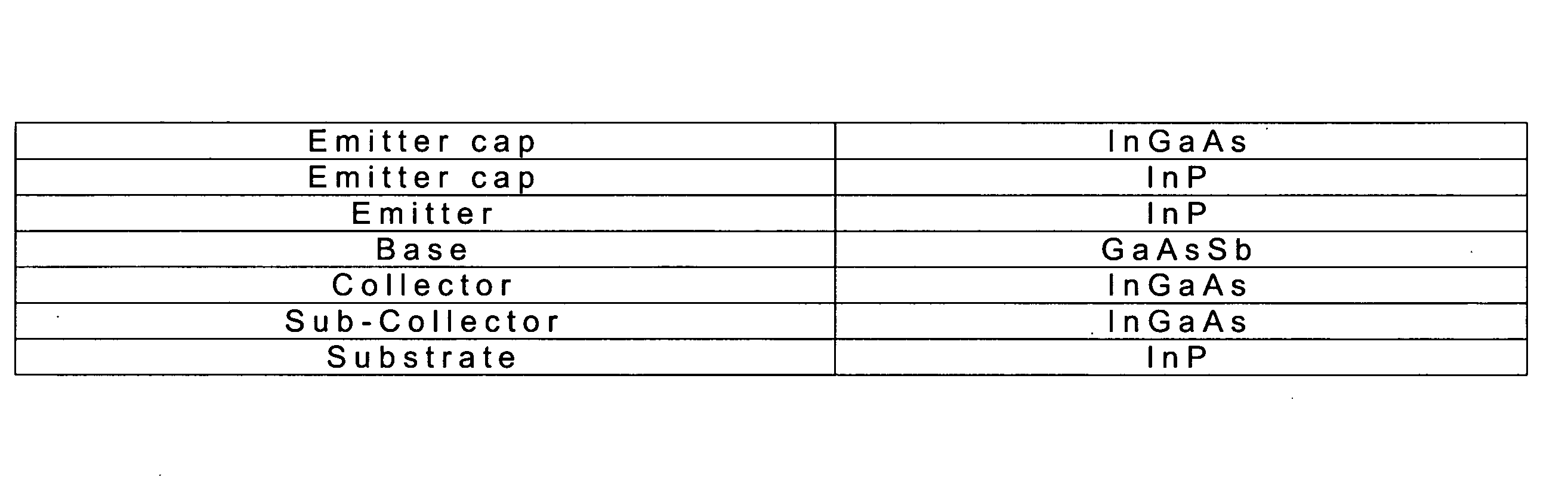
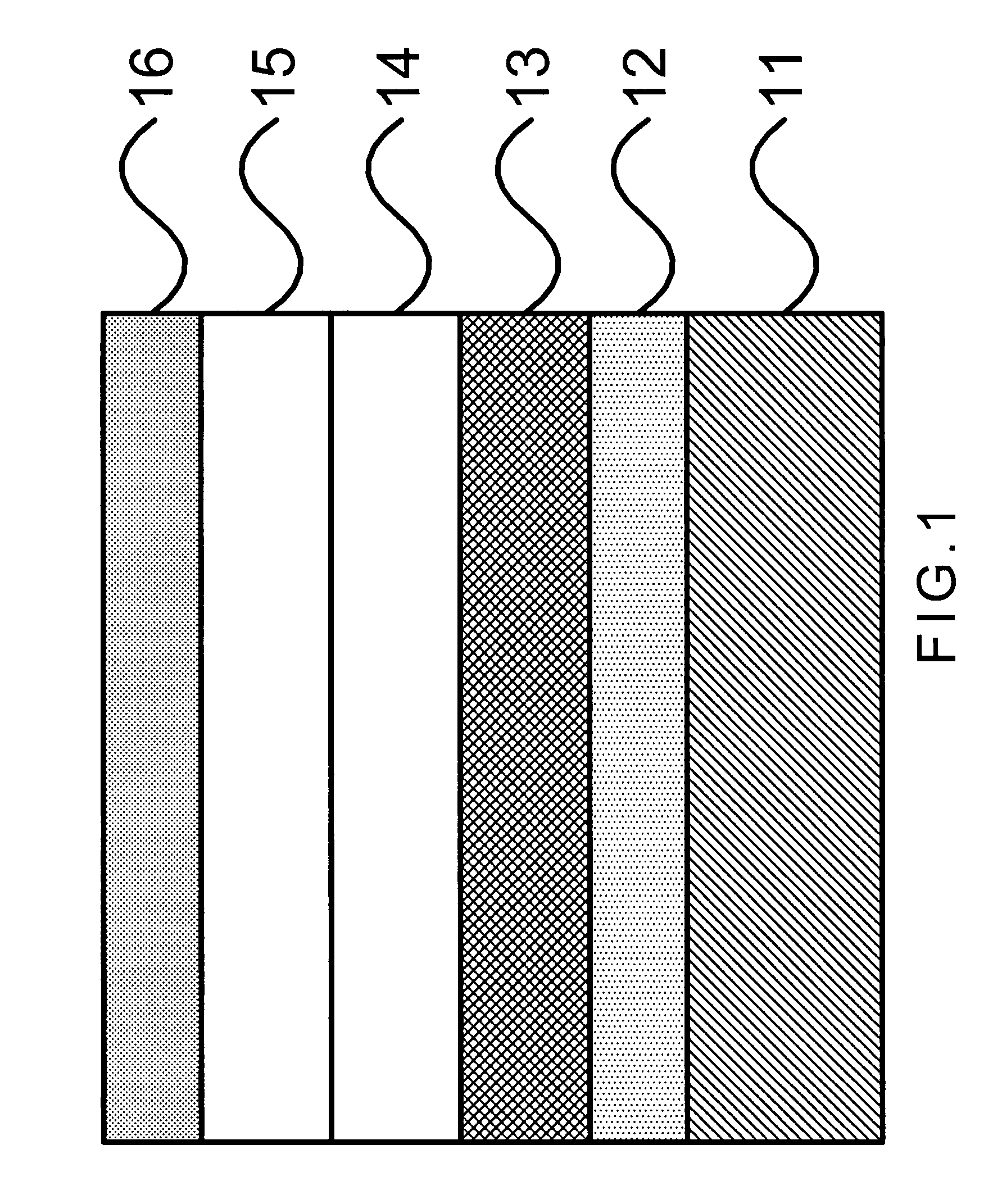
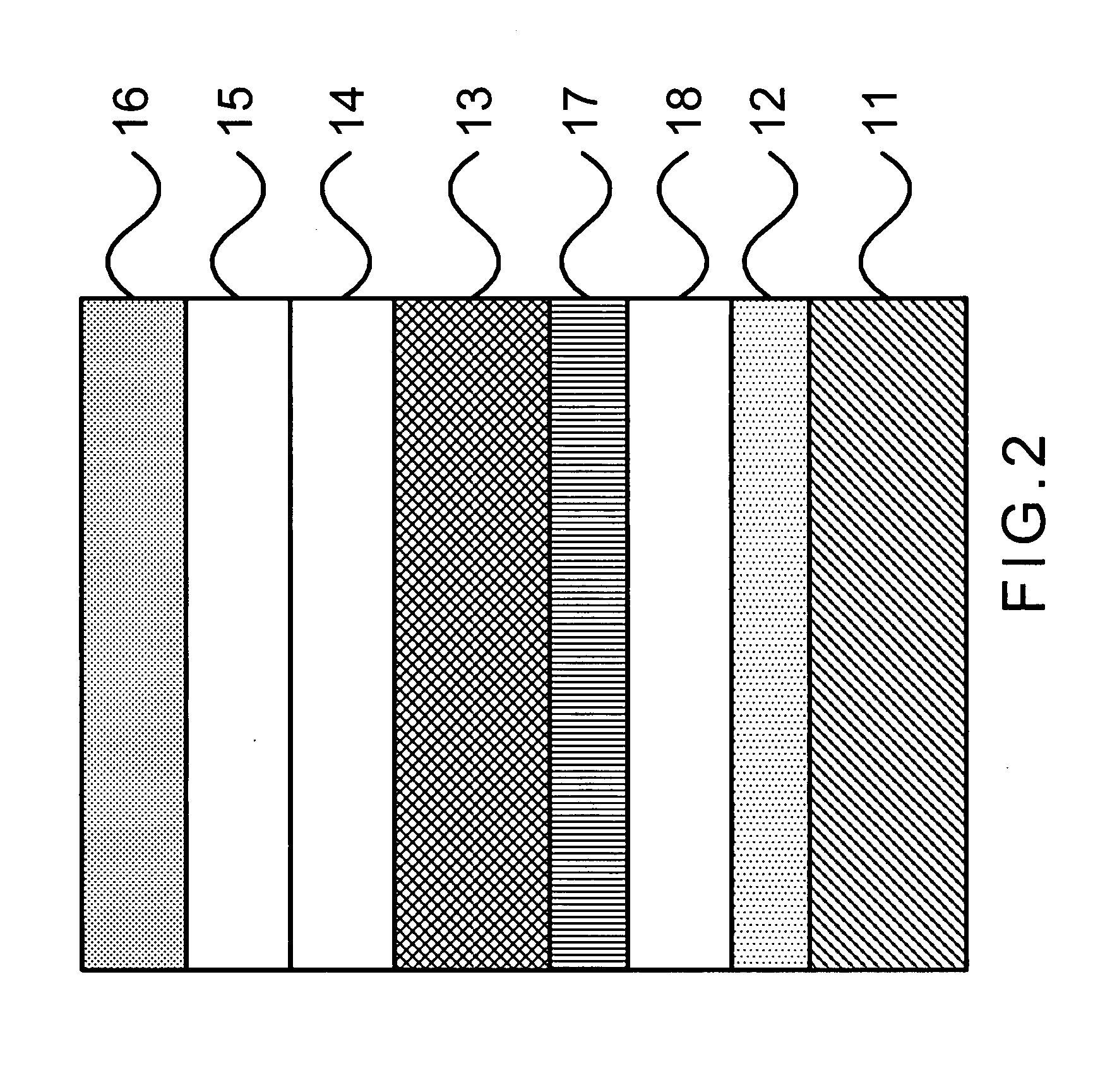
[0025]Please refer to FIG. 1 and FIG. 2, which are structural views showing a heterojunction bipolar transistor (HBT) having an (In)(Al)GaAsSb / InGaAs base-collector structure; and the HBT further comprising a second collector structure and a third collector structure according to the present invention. As shown in the figures, the present invention is an HBT having an (In)(Al)GaAsSb / InGaAs base-collector structure, comprising a substrate 11, a sub-collector contact layer 12, a first collector structure 13, a base structure 14, an emitter structure 15 and an emitter contact layer 16.
[0026]As shown in FIG. 2, a second collector structure 17 and a third collector structure 18 are added between the first collector structure 13 and the sub-collector contact layer 12.
[0027]The base structure 14 is grown on the first collector structure 13 throug...
PUM
 Abstract
Description
Claims
Application Information