

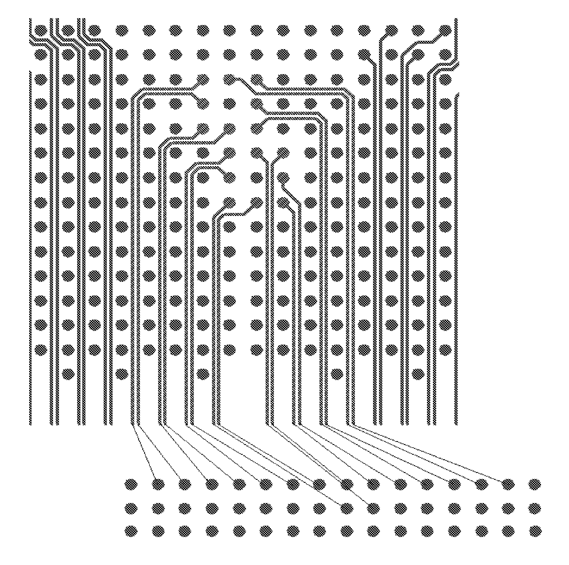
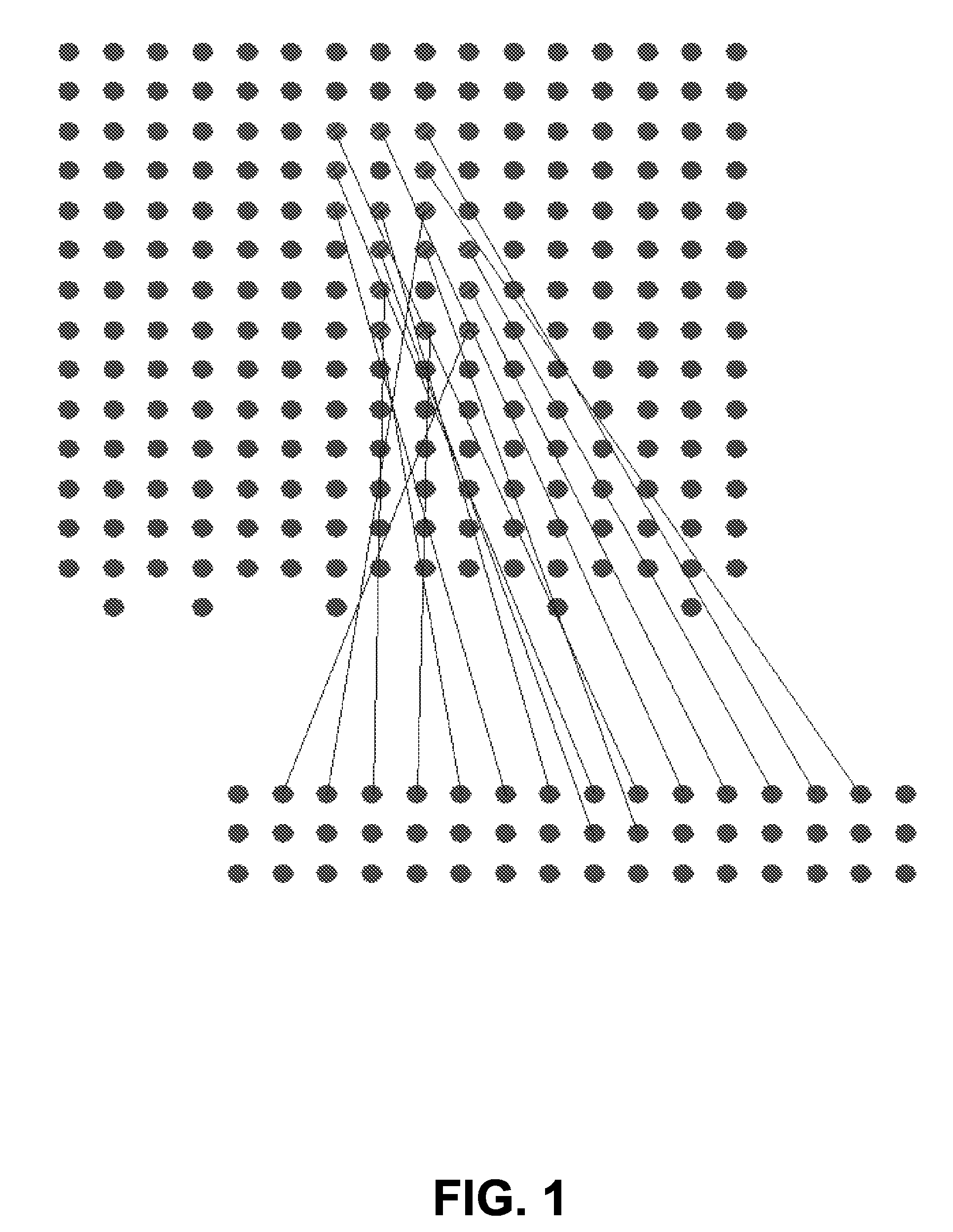
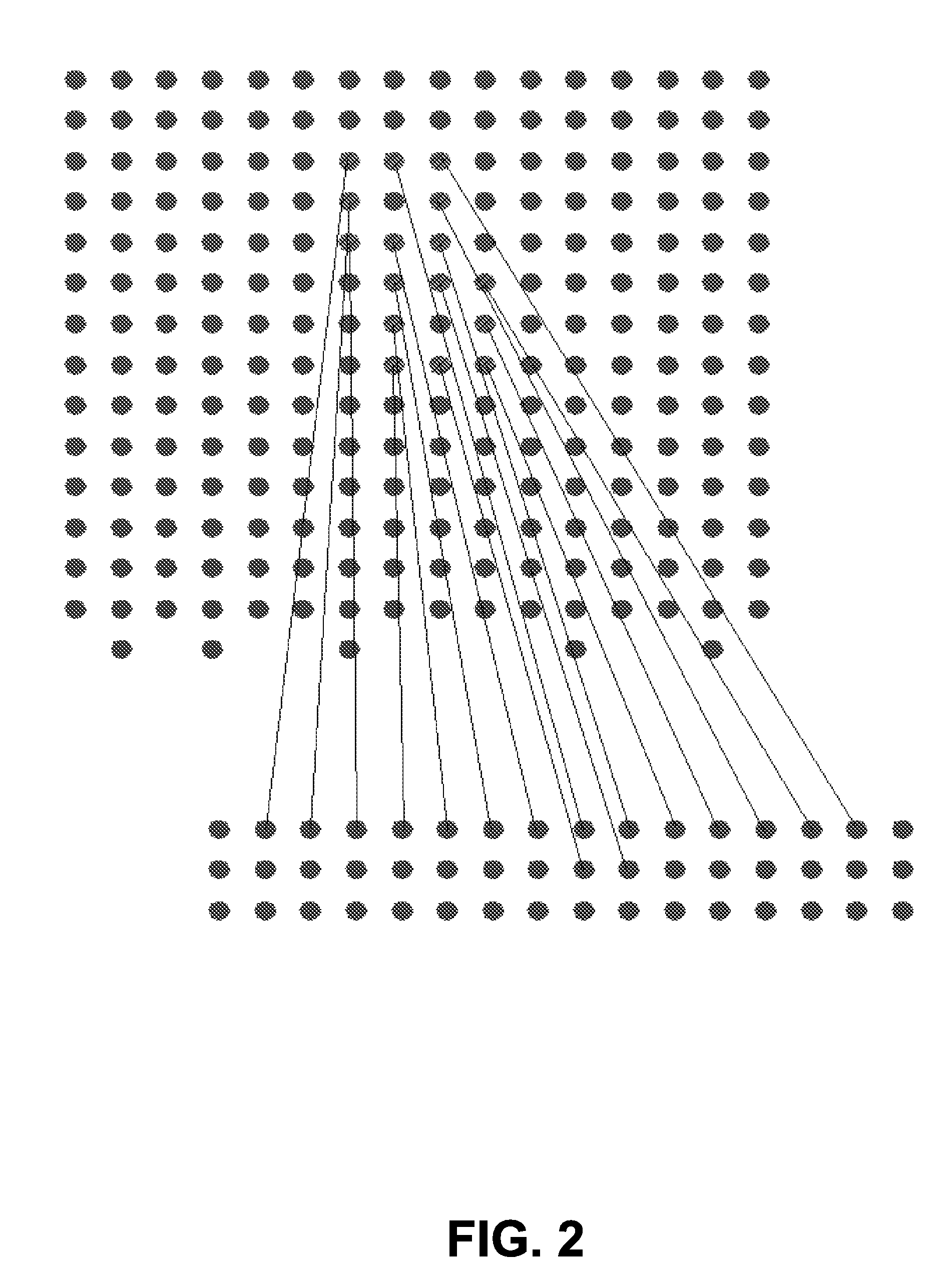
Use of breakouts in printed circuit board designs
a technology of printed circuit boards and breakouts, applied in the direction of cad circuit design, program control, instruments, etc., can solve the problems of limiting the length and/or impedance of a trace, constraints restricting the designer's ability to route the traces, and more complex printed circuit boards, etc., to achieve the effect of improving the creation of escape traces
- Summary
- Abstract
- Description
- Claims
- Application Information
AI Technical Summary
Benefits of technology
Problems solved by technology
Method used
Image

Examples
Embodiment Construction
[0036]As will be appreciated by those of ordinary skill in the art, printed circuit board design tools are conventionally implemented using computer-executable software instructions executed by one or more programmable computing devices. Accordingly, one or more aspects of the invention may be embodied by the execution of software instructions on a programmable computing device to perform one or more functions according to the invention. Alternately or additionally, one or more aspects of the invention may be embodied by computer-executable software instructions stored on a computer-readable medium for performing one or more functions according to the invention. Accordingly, the components and operation of a generic programmable computer system through which various embodiments of the invention may be employed will first be described with reference to FIG. 7. It should be noted that this operating environment is only one example of a suitable operating environme...
PUM
 Abstract
Description
Claims
Application Information