Thin film transistor, method of producing the same, and display device using the thin film transistor

a thin film transistor and transistor technology, applied in the direction of semiconductor devices, basic electric elements, electrical appliances, etc., can solve the problems of more serious problems, disadvantageous miniaturization and high resolution of processes, etc., to enhance the liability of thin film transistors, reduce the layout area of polycrystalline semiconductor films, improve the dielectric strength of gate insulating films

Inactive Publication Date: 2008-07-31
MITSUBISHI ELECTRIC CORP
View PDF12 Cites 8 Cited by
  • Summary
  • Abstract
  • Description
  • Claims
  • Application Information

AI Technical Summary

Benefits of technology

[0017]According to the thin film transistor of the invention, at least in a region where a polycrystalline semiconductor film intersects with a gate electrode, a pattern end portion of the polycrystalline semiconductor film has a small taper angle. Therefore, the covering property of a gate insulating film formed on the surface of the portion is sufficiently ensured. In a region where the polycrystalline semiconductor film does not intersect with a gate electrode, the tapered shape due to resist withdrawal is suppressed. Therefore, the layout area of the polycrystalline semiconductor film can be reduced. Consequently, effects that the dielectric strength of a gate insulating film of a thin film transistor is improved to enhance there liability of the thin film transistor, and that the layout area is reduced to miniaturize the thin film transistor, thereby obtaining a high-resolution display device. The invention can be applied not only to a liquid crystal display device, but also to an active matrix display device such as an EL display device.

Problems solved by technology

In the process using the resist withdrawal method, all pattern end portions of a polycrystalline semiconductor film are processed into a tapered shape, and hence there is the following problem.
Therefore, the process is disadvantageous in miniaturization and high resolution.
This problem is more serious in the case where portions where a tapered shape is necessary, and those where a tapered shape is unnecessary in order to put priority on miniaturization mixedly exist.

Method used


Image

  • Thin film transistor, method of producing the same, and display device using the thin film transistor
  • Thin film transistor, method of producing the same, and display device using the thin film transistor
  • Thin film transistor, method of producing the same, and display device using the thin film transistor

Examples


embodiment 1

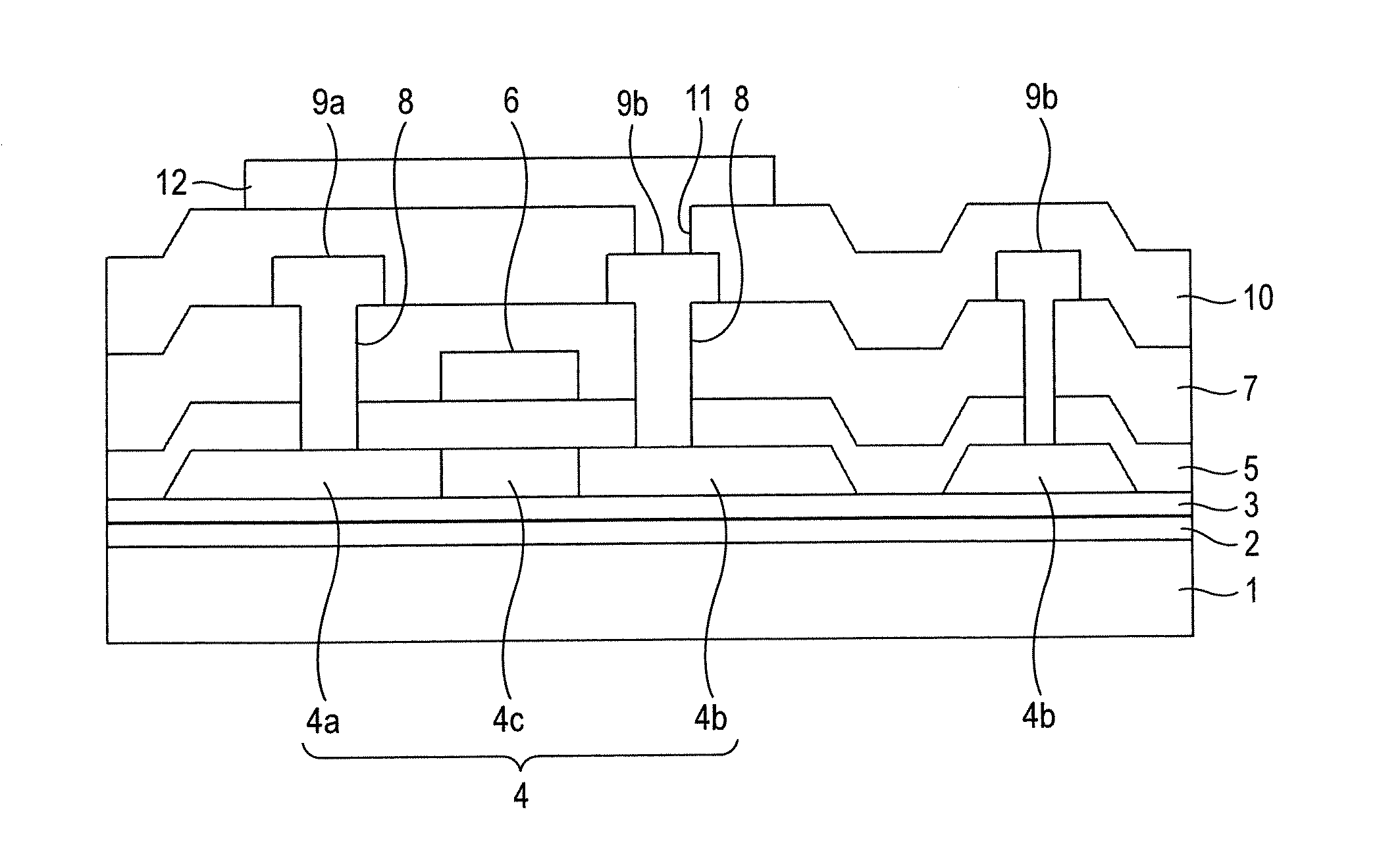
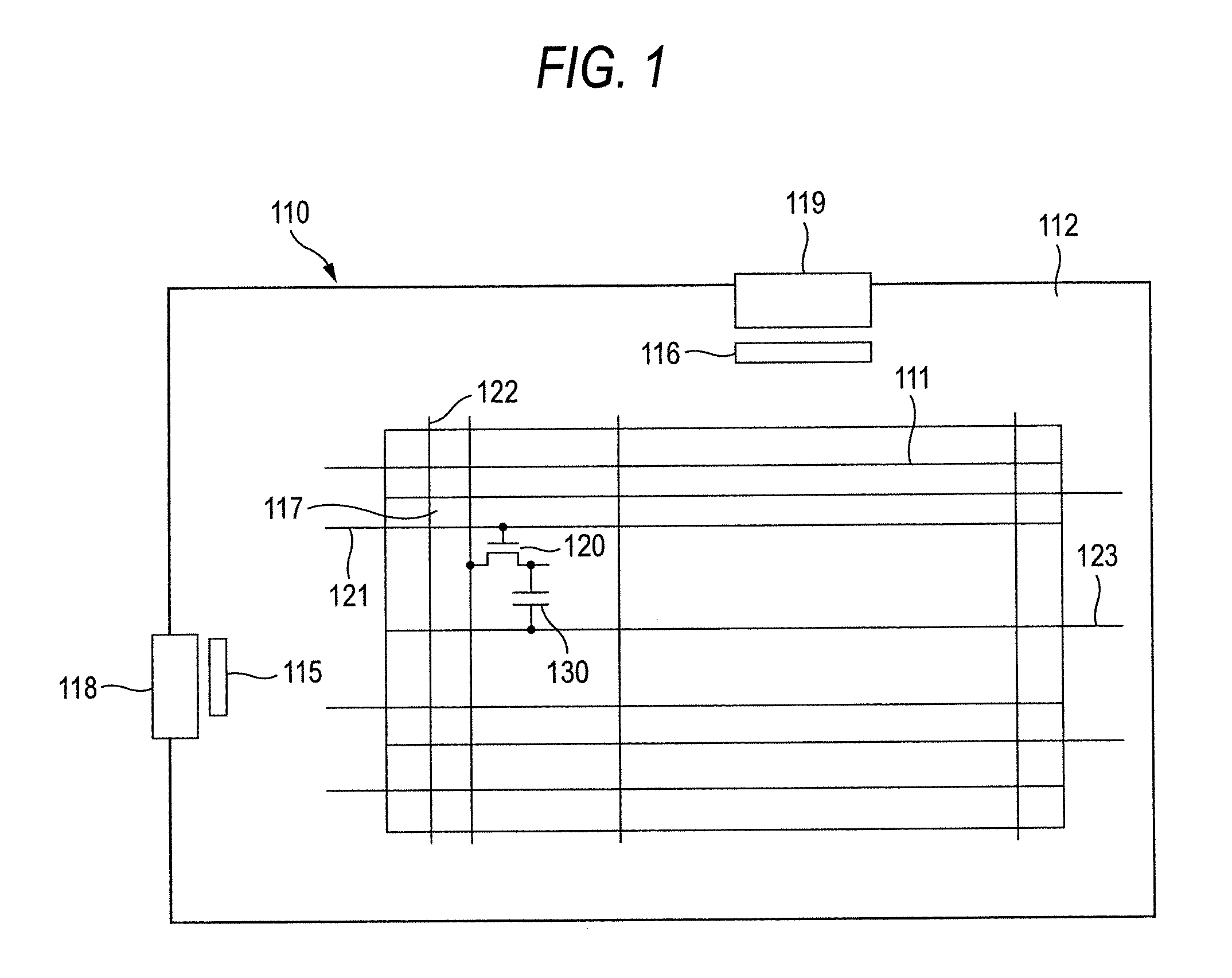
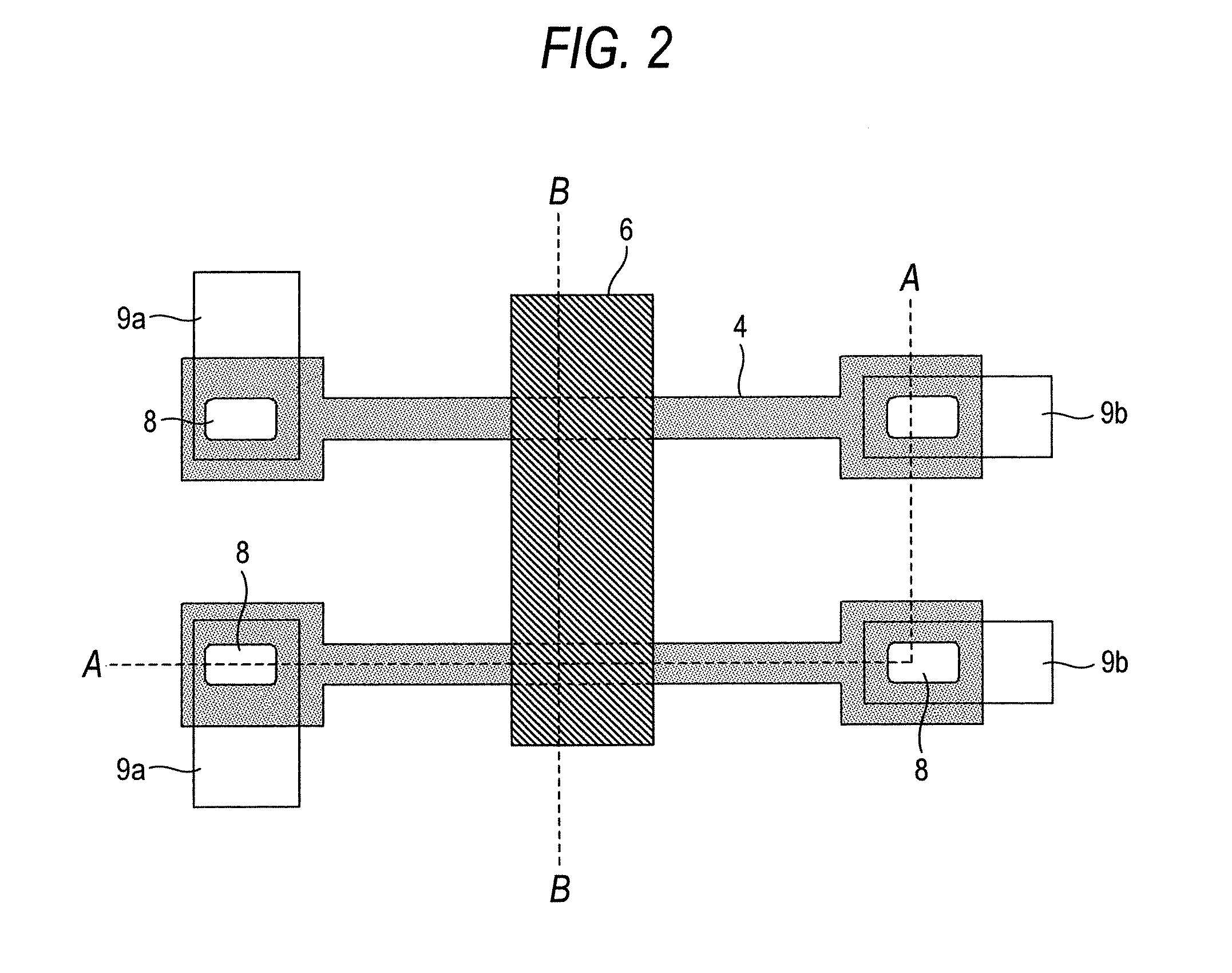
[0029]First, an active matrix display device to which a TFT substrate of the invention is applied will be described with reference to FIG. 1. FIG. 1 is a front view showing the configuration of a TFT substrate used in the display device. As the display device of the invention, a liquid crystal display device will be exemplarily described. However, this is for illustrative purpose only. Alternatively, for example, a flat panel display device such as an organic EL display device may be used.

[0030]The display device of the invention has the TFT substrate 110. For example, the TFT substrate 110 is a TFT array substrate. In the TFT substrate 110, a display region 111, and a frame region 112 which surrounds the display region 111 are disposed. In the display region 111, plural gate wirings (scan signal lines) 121 and plural source wirings (display signal lines) 122 are formed. The gate wirings 121 are disposed in parallel to one another. Similarly, the source wirings 122 are disposed in p...


PUM


Abstract

It is an object to obtain a display device which has a thin film transistor using a semiconductor film, and in which initial failures are reduced, and a high-resolution display due to miniaturization of the thin film transistor is enabled. In a thin film transistor, a gate electrode 6 is formed above a polycrystalline semiconductor film 4 via a gate insulating film 5. A taper angle θ2 of a section of a pattern end portion of the polycrystalline semiconductor film 4 in a region where the polycrystalline semiconductor film 4 and the gate electrode 6 intersect with each other is smaller than a taper angle θ1 of the other region.

Description

CROSS-REFERENCE TO RELATED APPLICATION[0001]This application is based upon and claims the benefit of priority from Japanese Patent Application No. 2007-021364 filed on Jan. 31, 2007, the entire contents of which are incorporated herein by reference.BACKGROUND OF THE INVENTION[0002]1. Field[0003]The present invention relates to a thin film transistor, a method of producing it, and a display device using it.[0004]2. Description of the Related Art[0005]A liquid crystal display device (LCD) which is one of conventional usual thin panels is generally used as a monitor for a personal computer, that for portable information terminal, and the like, while taking advantage of low power consumption, small size, and lightweight. Recently, the liquid crystal display device (LCD) is widely used in a TV set, and will replace a conventional cathode-ray tube. In addition, an electroluminescence EL display device in which a luminous body such as an EL element is employed in a pixel display portion is...

Claims


Application Information

Patent Timeline
Patent Type & Authority Applications(United States)
IPC IPC(8): H01L29/10H01L21/00
CPCH01L29/66757H01L29/78675H01L29/78606H01L29/42384H01L29/78618
Inventor TAKEGUCHI, TORU
Owner MITSUBISHI ELECTRIC CORP
Why Eureka
Try Eureka