
Resistor element and manufacturing method thereof

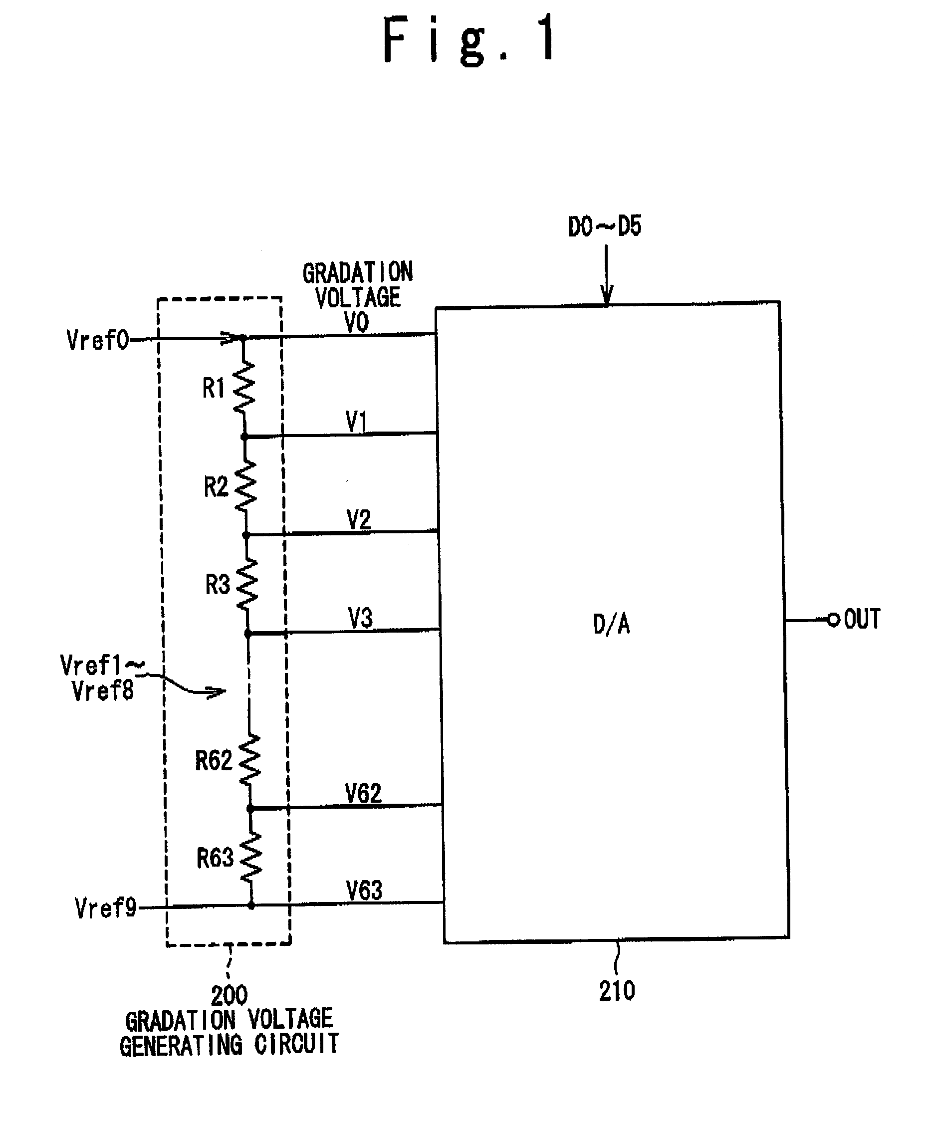
a technology of resistor elements and manufacturing methods, which is applied in the direction of semiconductor devices, semiconductor/solid-state device details, electrical devices, etc., can solve the problems of difficult control of thickness and the area failure of gradation display, and difficulty in forming a uniform thickness of the silicide layer, so as to improve the product liability

Inactive Publication Date: 2007-05-31
NEC ELECTRONICS CORP
View PDF5 Cites 0 Cited by
  • Summary
  • Abstract
  • Description
  • Claims
  • Application Information

AI Technical Summary

Benefits of technology

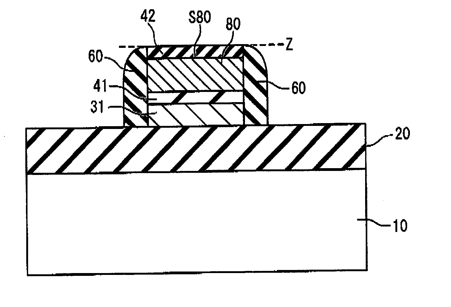
[0013] In a first aspect of present invention, a manufacturing method of a resistor element is provided. The manufacturing method includes; (A) forming a polysilicon structure 50 whose top layer is a polysilicon layer 30, 32 on a substrate 10; (B) forming a metal layer 70 on the polysilicon layer 30, 32; (C) forming an upper barrier layer 42 on the metal layer 70; and (D) forming a silicide layer 80 whose upper surface S80 is covered with the upper barrier layer 42 after the process (C) through a reaction between the polysilicon layer 30,32 and the metal layer 70. Therefore, it becomes possible to control a grain growth in an upward direction during the silicidation and suppress a variation in a thickness of the silicide layer 80, i.e., a variation of the resistive element.
[0014] The present invention preferably includes following processes between the process (A) and (B); (E) forming a sidewall 60 on a side of the polysilicon structure 50; and (F) removing a portion of the polysilicon layer 30,32 after the process (E) to form a space surrounded by an upper surface 830,32 of the polysilicon structure 50 and the sidewall 60. In this case, the metal layer 70 is formed in the space during the step (B). The silicide layer 80 is formed so that a side thereof is surrounded by the sidewall 60 during the process (D). Therefore, it becomes possible to control a grain growth in a side direction during the silicidation and suppress a variation in an area size of the silicide layer 80, i.e, a variation in a resistor element.
[0015] Further preferably, the process (A) includes: (a1) forming a lower polysilicon layer 31 on the substrate 10, (a2) forming a lower barrier layer 41 on the lower polysilicon layer 31, and (a3) forming an upper polysilicon layer 32 on the lower barrier layer 41 as the polysilicon layer. In this case, during the process (D), the silicide layer 80 is formed so that an upper surface thereof and bottom thereof are covered with the barrier layer 42, 41 respectively. Therefore, it becomes possible to control a grain growth in upward and downward direction during the silicidation and suppress the variation in a thickness of silicide layer 80, i.e, the variation in the resistor element.
[0017] According to the resistor element and the manufacturing method of the present invention, a grain growth in the silicidation is controlled. As a result, the variation of the area size and the thickness of a silicide layer which is formed are controlled. Therefore, the resistance variation in the silicide layer is controlled and the variation in the resistance of the whole resistor elements is also controlled. This leads to an improvement in there liability of the product employing the resistor element as a part of circuit.

Problems solved by technology

Here, since the silicidation progresses rapidly, generally it is difficult to form a silicide layer of uniform thickness.
However, since the silicidation progresses rapidly, it is difficult to control the thickness and the area of the silicide layer.
The variation in the silicide layers causes variation in the resistances of the polysilicon resistors, thereby causing a fault in gradation display as a result.

Method used


Image

  • Resistor element and manufacturing method thereof
  • Resistor element and manufacturing method thereof
  • Resistor element and manufacturing method thereof

Examples


first embodiment

1. First Embodiment

1-1. Structure

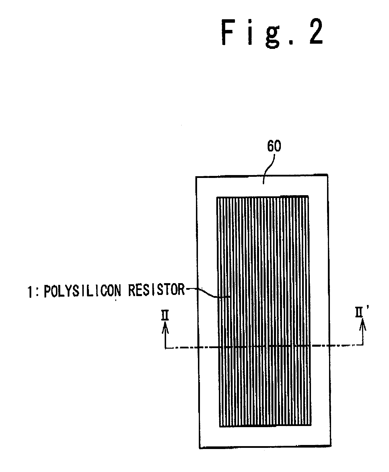
[0025]FIG. 2 is a plan view illustrating the structure of the resistor element of the first embodiment. The resistor element according to the present embodiment is provided with a polysilicon resistor 1 which has a predetermined area within a plane. The polysilicon resistor 1 is surrounded by a sidewall 60 in the plane. The sectional view along the line II-II′ in the figure is shown in FIG. 3.

[0026] As shown in FIG. 3, an element separation structure 20 is formed into a substrate 10. The substrate 10 is a P-type silicon substrate, for example. The element separation structure 20 is STI (Shallow Trench Isolation) structure or LOCOS (LOCal Oxidation of Silicon) structure. Furthermore, the structure corresponding to the polysilicon resistor 1 is formed in a predetermined position on the substrate 10. Specifically, a polysilicon layer 31 is formed on the substrate 10 (element separation structure 20), a lower barrier layer 41 is formed on the polysili...

second embodiment

2. Second Embodiment

[0051] In a second embodiment of the present invention, the structure where the upper barrier layer 42 is eliminated from the resistor element according to the above mentioned first embodiment is described. Referring to FIGS. 5A-5D, the manufacturing process of the resistor element according to the present embodiment is described. The explanations which already have described in the first embodiment are suitably omitted for avoiding redundant description.

[0052] After the process shown in FIGS. 4A-4F is completed, the metal layer 70 for the silicidation is formed on the surface of the upper polysilicon layer 32. As a result, a structure shown in FIG. 5A is obtained. The metal layer 70 is a Ti film with the thickness of 200 A, for example. This metal layer 70 is formed so that the upper surface S70 will be lower than the topmost part Z of the sidewall 60.

[0053] Subsequently, a heat treatment is performed and the silicidation occurs between the upper polysilicon l...

third embodiment

3. Third Embodiment

[0058] In a third embodiment of the present invention, the structure where the lower barrier layer 41 is eliminated from the resistance element according to the above-mentioned first embodiment is provided. Referring to FIGS. 6A-6E, the manufacturing process of the resistance element according to the present embodiment is explained. The explanations which already have described in the first embodiment are suitably omitted for avoiding redundant description.

[0059] First, as shown in FIG. 6A, the polysilicon structure including a polysilicon layer 30 with the thickness of about 1500 A is formed on the substrate 10 (element separation structure 20). The sidewall 60 is formed in on both sides of the polysilicon structure. The sidewall 60 is formed for surrounding all the sides of the polysilicon layer 30.

[0060] Subsequently, the polysilicon layer 30 is selectively etched about 500 A.

[0061] This is realizable by the selectivity etching or the etching employing the p...


PUM

PropertyMeasurementUnit
resistivityaaaaaaaaaa
depthaaaaaaaaaa
resistanceaaaaaaaaaa

Abstract

A method of manufacturing a resistive element of present invention comprises; (A) forming on a substrate, a polysilicon structure whose top layer is a polysilicon layer; (B) forming a metal layer on the polysilicon layer; (C) forming an upper barrier layer on the metal layer; and (D) forming a silicide layer whose surface is covered with the upper barrier layer after the process (C) through a reaction between the polysilicon layer and the metal layer. According to the present invention, a variation in a resistor element of a semiconductor device can be suppressed.

Description

BACKGROUND OF THE INVENTION [0001] 1. Field of the Invention [0002] The present invention relates to a resistor element in a semiconductor device and a manufacturing method thereof. Particularly, the present invention relates to a resistor element having silicide, and a manufacturing method thereof. [0003] 2. Description of the Related Art [0004] The influence of a resistance of a gate electrode or source and drain electrodes upon a processing speed of device becomes remarkable with minimizing of a MOS transistor. In order to reduce the resistivity of these electrodes, a technology using silicide is conventionally known (for example, see Japanese Laid Open Patent Application (JP-P 2001-223177A) and Japanese Laid Open Patent Application (JP-A-Heisei 7-201775)). The gate electrode to which the silicide technology is applied has a polycide structure which includes a polysilicon layer and a silicide layer. The silicide layer is formed by the silicidation process between a polysilicon fi...

Claims


Application Information

Patent Timeline
Patent Type & Authority Applications(United States)
IPC IPC(8): H01L23/62H01L21/20
CPCH01L23/5228H01L27/0802H01L28/24H01L2924/0002H01L2924/00
Inventor NAGAI, TAKAYUKI
Owner NEC ELECTRONICS CORP
Learn More