

UV curing of pecvd-deposited sacrificial polymer films for air-gap ild
a technology of sacrificial polymer films and air gaps, which is applied in the direction of basic electric elements, electrical equipment, semiconductor devices, etc., can solve the problems of increasing the demands on processing techniques and physical characteristics, affecting the functioning of the system, and the individual features of the system continue to decreas
- Summary
- Abstract
- Description
- Claims
- Application Information
AI Technical Summary
Benefits of technology
Problems solved by technology
Method used
Image

Examples
Embodiment Construction
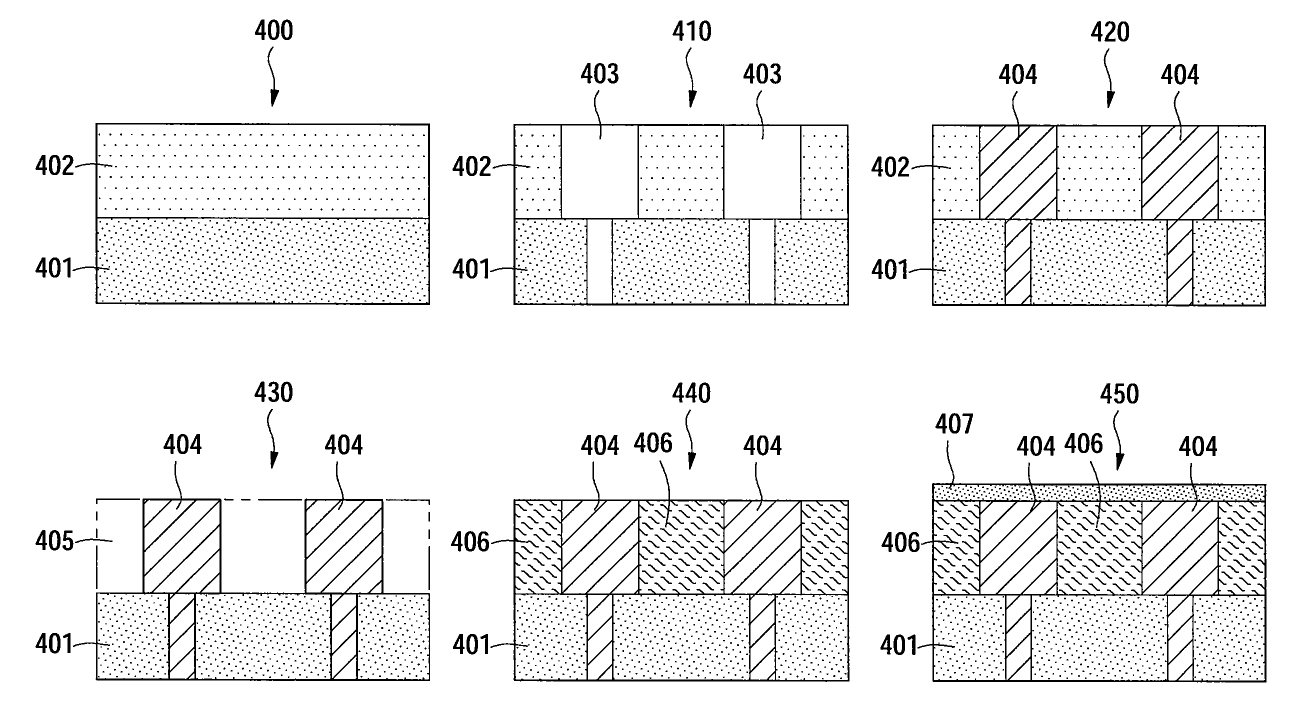
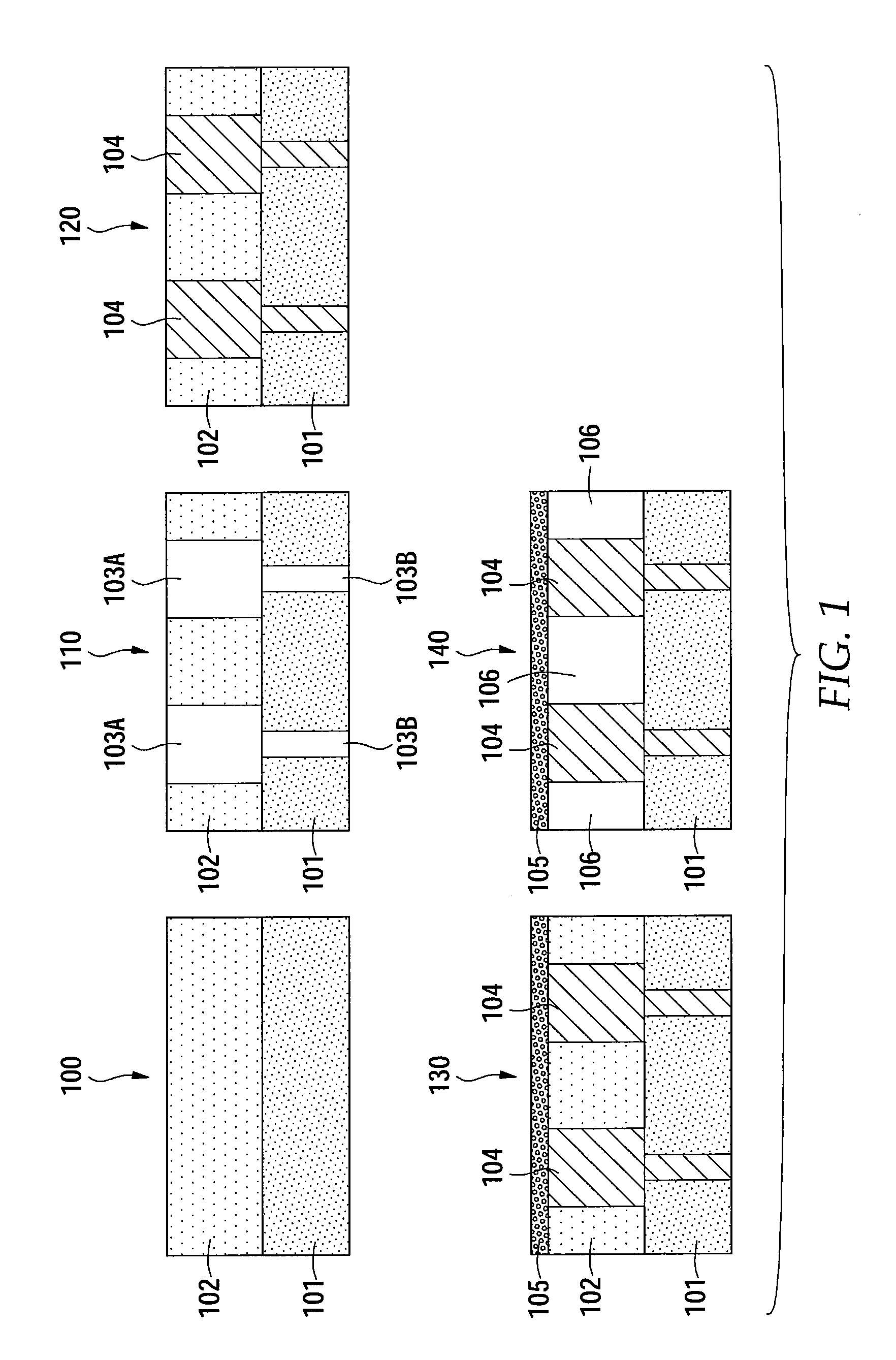
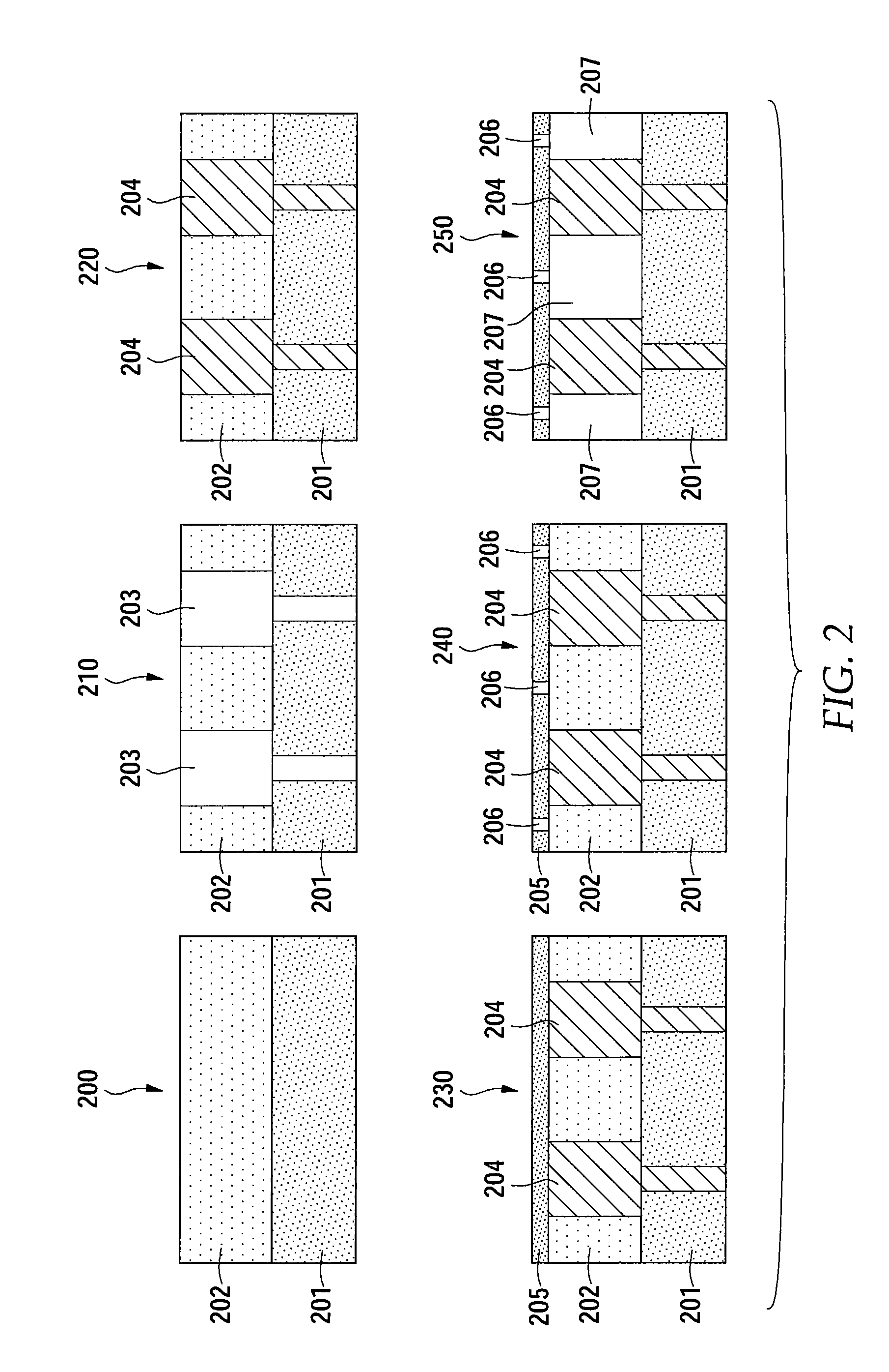
[0020]In certain embodiments a method for forming an air gap between conductive elements of a semiconductor device is generally provided. The air gap is generally formed by depositing a removable material between the conductive elements, depositing a porous layer over the removable material and the conductive elements, and then stripping the deposited material out of the space between the conductive elements through the porous layer to leave an air gap between the conductive elements. Although removable materials are discussed with reference to alpha terpinine, it should be understood that the exemplary methods described herein may be performed using other removable materials such as poly(methyl methacrylate) or parylenes.
[0021]Certain embodiments may be practiced on any plasma enhanced CVD chamber or system including systems such as the CENTURA ULTIMA HDP-CVD™ system, PRODUCER APF PECVD™ system, PRODUCER BLACK DIAMOND™ system, PRODUCER BLOK PECVD™ system, PRODUCER DARC PECVD™ syste...
PUM
 Abstract
Description
Claims
Application Information