Pattern forming method and pattern verifying method

a technology of pattern and forming method, applied in the direction of computer aided design, program control, instruments, etc., can solve the problems of inability to detect the danger of pattern and layout being modified by an unnecessarily large amount of modification, and inability to verify whether input design data is correctly modified on the basis of a guidelin

Inactive Publication Date: 2008-07-31
KK TOSHIBA
View PDF21 Cites 23 Cited by
  • Summary
  • Abstract
  • Description
  • Claims
  • Application Information

AI Technical Summary

Problems solved by technology

Accordingly, when process simulation is performed on design data of a pattern designed in conformity with a design rule, although optical proximity correction (OPC), a resolution enhanced technology (RET) process and the like are performed, process dangerous portions where patterns are connected to each other or disconnected from each other at unexpected positions, or line widths or space widths of patterns not satisfying regulated conditions are occasionally found.
However, even though these verifying methods are used, it cannot be verified whether input design data is correctly modified on the basis of a guideline for modification.
More specifically, when a design rule check, process rule check and the like are performed, even though a modification result satisfies the design rule and passes these checks and the predicted process dangerous portions are eliminated, it is impossible to detect the danger that the pattern and the layout might be modified by an unnecessarily large amount of modification in comparison with the pattern and the layout intended by a designer.
Since a design target itself is modified by the above modification method, verification performed by “comparison with target” as a general verification cannot be performed, and the propriety of the modification cannot be easily verified.
As a result, when a portion which is unexpectedly modified or a portion which is fatally modified is not detected by the process rule check, the modified portions cannot be detected.
In this manner, according to a conventional technique, when design data and a design layout of a pattern initially input in a pattern design process are unexpectedly modified, these modified portions cannot be automatically detected.
The pattern design process thus requires a lot of time and enormous cost.
In addition, since criteria for determining pseudo errors and true errors depend on the verifier, mask data having uniform quality cannot be easily created.

Method used


Image

  • Pattern forming method and pattern verifying method
  • Pattern forming method and pattern verifying method
  • Pattern forming method and pattern verifying method

Examples


first embodiment

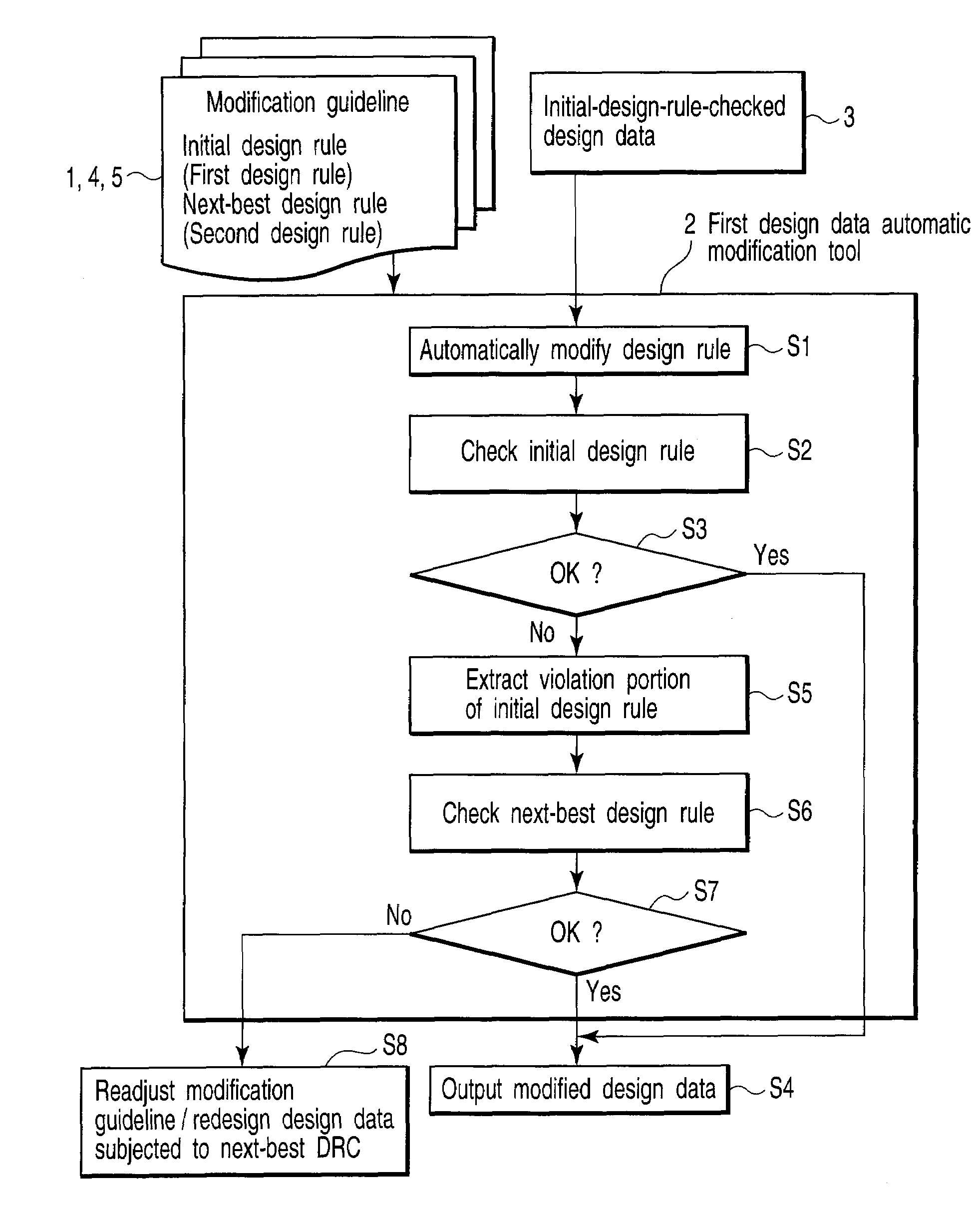
[0024]A first embodiment according to the present invention will be described below with reference to FIGS. 1 and 2. In the first embodiment, the following technique will be described. That is, when a process dangerous portion of a pattern is automatically modified prior to actual formation of the pattern to be formed in a semiconductor device, the propriety of design data at the portion modified while partially outstripping a design rule is automatically checked without a manual operation to make it possible to efficiently check the modified portion. Accordingly, a technique which can easily create design data of a proper pattern including a modification which partially outstrips a design rule will be also described below.

[0025]A pattern forming method according to the embodiment will be described below with reference to a dangerous portion modifying flow according to the embodiment shown in FIG. 1.

[0026]As shown in FIG. 1, prior to execution of a pattern forming method according t...

second embodiment

[0071]A second embodiment according to the present invention will be described below with reference to FIGS. 3, 4, and 5. The same reference numerals as in the first embodiment denote the same parts in the second embodiment, and a description thereof will be omitted.

[0072]In the embodiment, in addition to the first and second design rules used in the first embodiment, a third design rule is used. The second embodiment will be described below in detail.

[0073]A pattern forming method according to the embodiment will be described below with reference to a dangerous portion modifying flow shown in FIG. 3. The pattern forming method according to the embodiment modifies the dangerous portion in conformity with a design rule, depending on the necessity of the design rule.

[0074]As shown in FIG. 3, prior to execution of the pattern forming method according to the embodiment, an initial design rule 1, design data 3 which is subjected to first design rule check by the initial design rule 1 and...

third embodiment

[0115]A third embodiment according to the present invention will be described below with reference to FIGS. 6, 7A, 7B, 7C, 8A, 8B, 9, and 10. The same reference numerals as in the first and second embodiments denote the same parts in the third embodiment, and a detailed description thereof will be omitted.

[0116]The embodiment relates to a technique that efficiently and easily forms an optimum design pattern on semiconductor manufacturing process parameters given in advance and, in particular, to a technique that verifies the propriety of a method of modifying an automatically modified pattern or layout and can improve the quality of design data of the pattern or the layout. The embodiment will be concretely described below in detail.

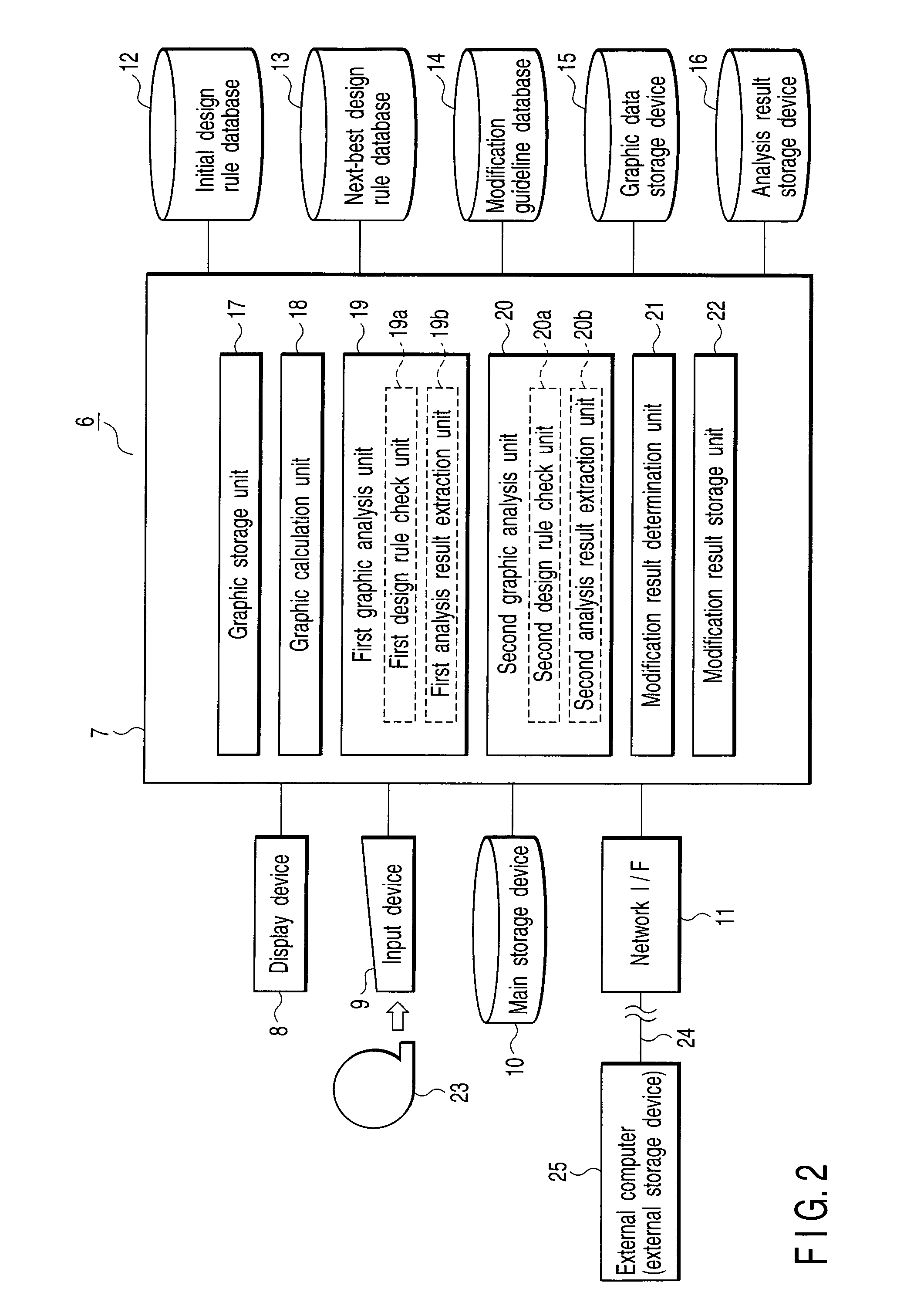
[0117]First, a pattern forming / verifying method according to the embodiment will be described below with reference to a flow of a verifying system for automatically modified design data shown in FIG. 6 and FIGS. 7A, 7B, 7C, 8A, and 8B. The pattern formin...


PUM


Abstract

A pattern forming method including modifying design data subjected to a first design rule check in design data of a pattern to be formed in a semiconductor substrate, performing the first design rule check to the modified design data again, outputting the modified design data which does not violate the first design rule as pattern forming design data used in actual pattern formation, and performing a second design rule check having an allowable range wider than that of the first design rule to the modified design data which violates the first design rule, and outputting the modified design data which does not violate the second design rule as the pattern forming design data, and redesigning the pattern to satisfy the second design rule or adjusting the modification guideline such that the modified design data which violates the second design rule satisfies the second design rule.

Description

CROSS-REFERENCE TO RELATED APPLICATIONS[0001]This application is based upon and claims the benefit of priority from prior Japanese Patent Application No. 2007-016707, filed Jan. 26, 2007, the entire contents of which are incorporated herein by reference.BACKGROUND OF THE INVENTION[0002]1. Field of the Invention[0003]The present invention relates to a technique of handling design data of a pattern of a semiconductor device and, more particularly, to a pattern forming method and a pattern verifying method which efficiently and uniformly process a series of processes according to data design of the pattern.[0004]2. Description of the Related Art[0005]In recent years, micropatterning and high integration density of a semiconductor device are conspicuous. Accordingly, when process simulation is performed on design data of a pattern designed in conformity with a design rule, although optical proximity correction (OPC), a resolution enhanced technology (RET) process and the like are perfor...

Claims


Application Information

Patent Timeline
Patent Type & Authority Applications(United States)
IPC IPC(8): G06F17/50
CPCG06F17/5081G06F30/398
Inventor KOBAYASHI, SACHIKO
Owner KK TOSHIBA
Why Eureka
Try Eureka