Pinned photodiode CMOS pixel sensor

a pixel sensor and photodiode technology, applied in the field of pinned photodiode cmos pixel sensor, can solve the problems of leakage current at the surface of silicon body, particularly troublesome problems,

Active Publication Date: 2008-08-07
FOVEON
View PDF11 Cites 23 Cited by
  • Summary
  • Abstract
  • Description
  • Claims
  • Application Information

AI Technical Summary

Problems solved by technology

One of the common problems associated with pixel sensors is leakage current at the surface of the silicon body in which the pixel sensors are fabricated.
This problem is particularly troublesome with respect to the blue detector, which is located at or near the silicon surface.

Method used


Image

  • Pinned photodiode CMOS pixel sensor
  • Pinned photodiode CMOS pixel sensor
  • Pinned photodiode CMOS pixel sensor

Examples


Embodiment Construction

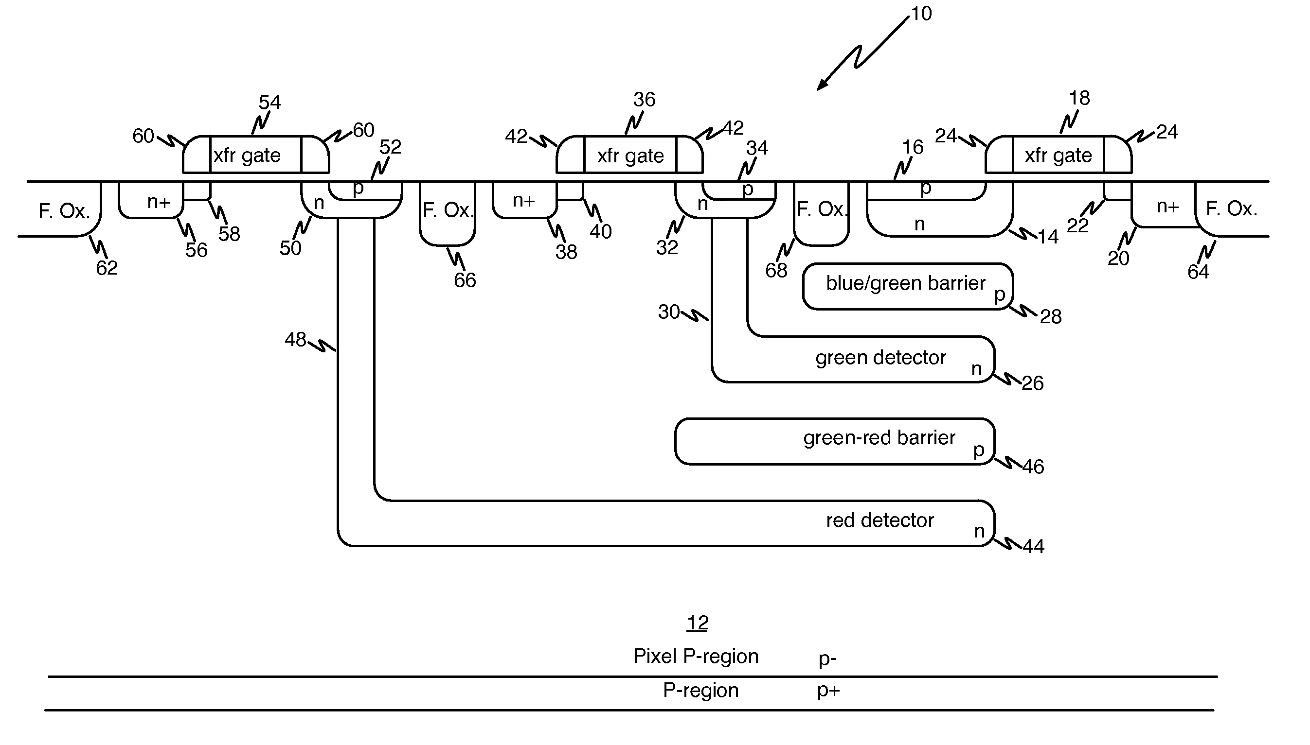
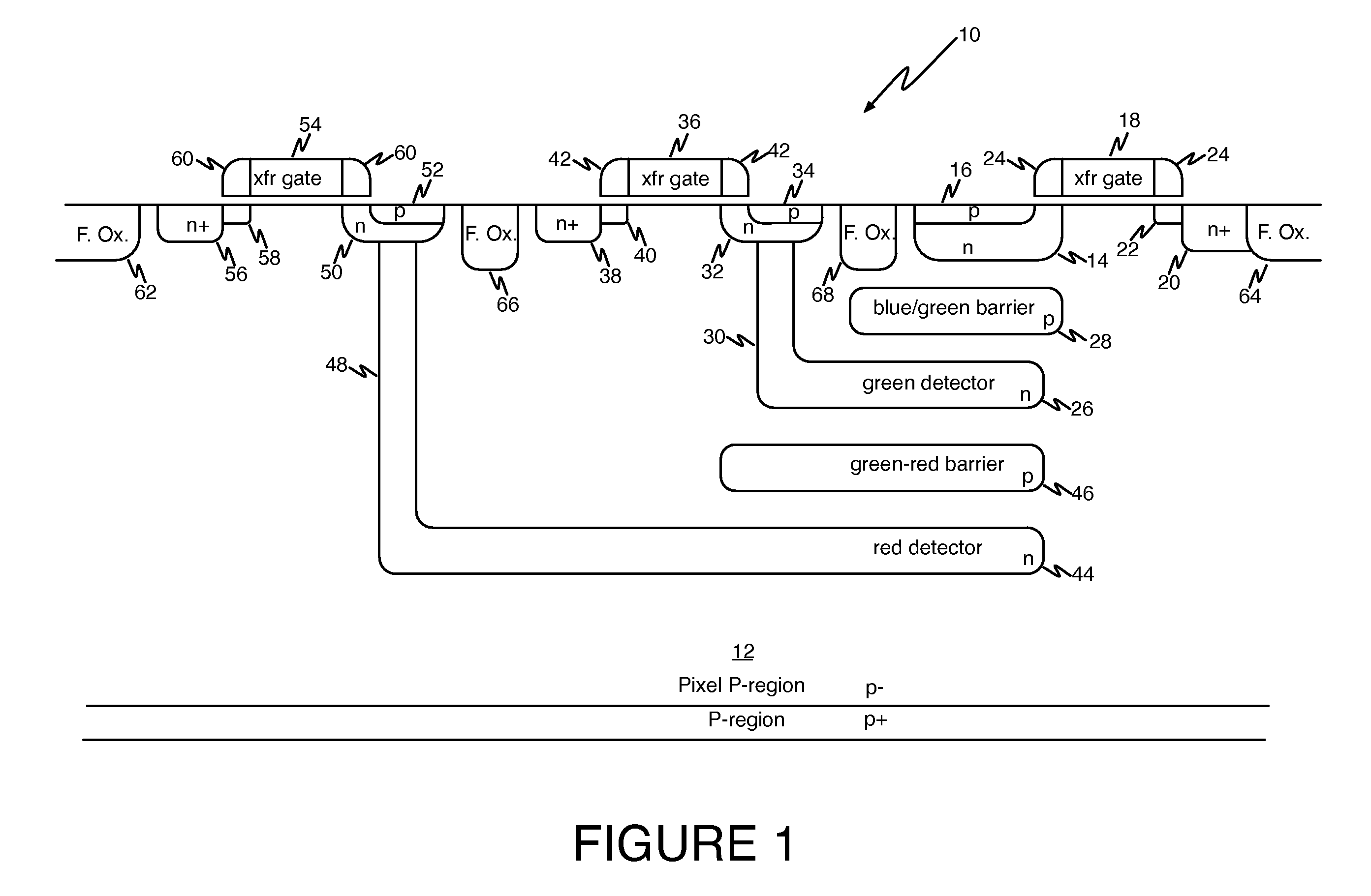
[0015]Persons of ordinary skill in the art will realize that the following description of the present invention is illustrative only and not in any way limiting. Other embodiments of the invention will readily suggest themselves to such skilled persons.

[0016]Referring first to FIG. 1, a multicolor CMOS pixel sensor 10 is formed in a p-type semiconductor region, preferably in a p-type region 12 formed in a semiconductor substrate. Persons of ordinary skill in the art will appreciate that the pixel sensor shown in the cross sectional view of FIG. 1 is illustrative only and that the relative locations of the semiconductor structures depicted therein have been selected to illustrate the structures rather than to provide a layout for an actual integrated circuit employing the pixel sensor of the present invention. Such skilled persons will also appreciate that the pixel sensor depicted in FIG. 1 could also be formed directly in a p-type substrate.

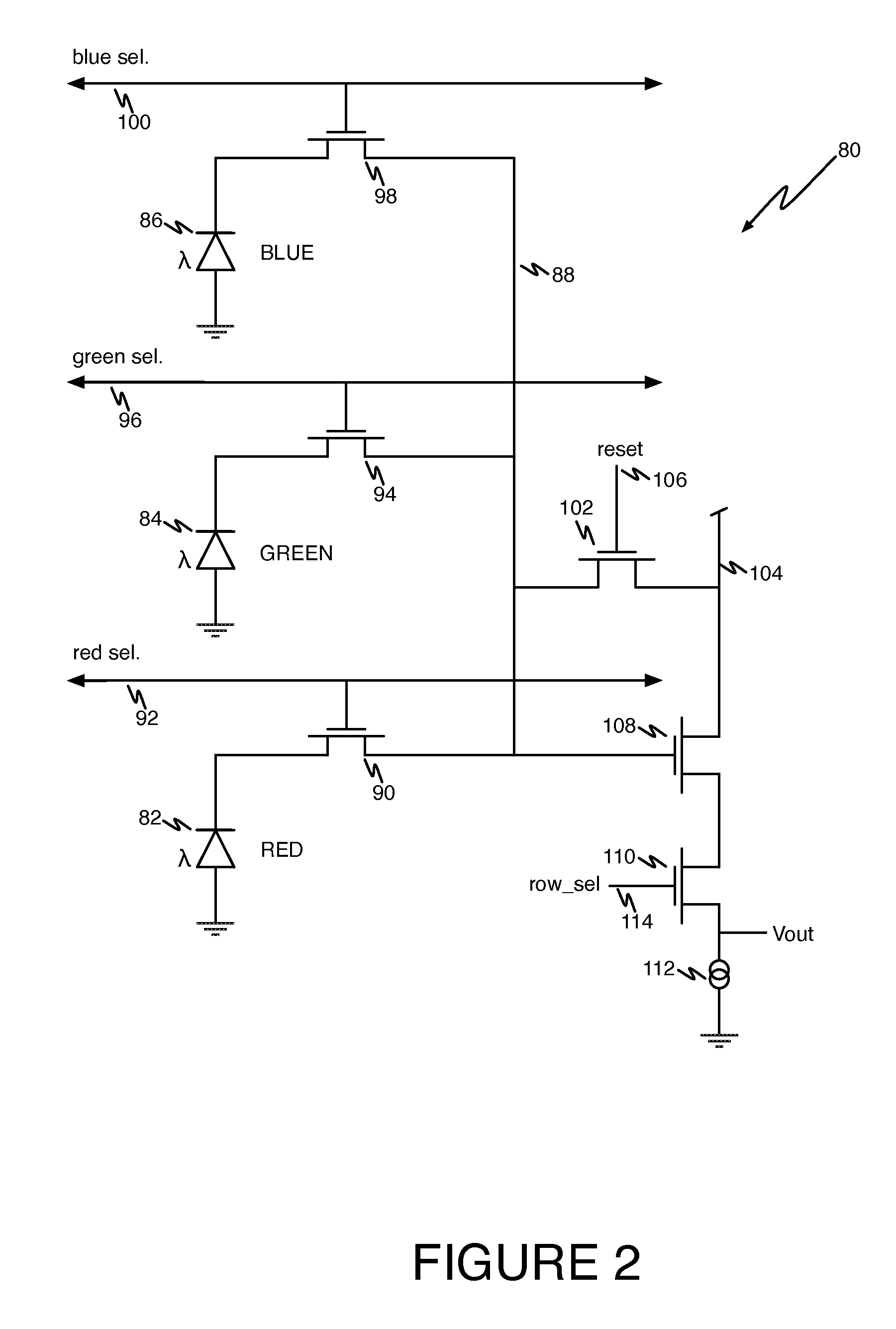
[0017]The multicolor CMOS pixel sensor 10...


PUM


Abstract

A multicolor CMOS pixel sensor formed in a p-type semiconductor region includes a first detector formed from an n-type region of semiconductor material located near the surface of the p-type region. A first pinned p-type region is formed at the surface of the p-type region over the first detector, and has a surface portion extending past an edge of the pinned p-type region. A second detector is formed from an n-type region located in the p-type semiconductor region below the first detector. A second-detector n-type deep contact plug is in contact with the second detector and extends to the surface of the p-type semiconductor region. A second pinned p-type region is formed at the surface of the p-type semiconductor region over the top of the second-detector n-type deep contact plug. A surface portion of the second-detector deep contact plug extends past an edge of the second pinned p-type region.

Description

BACKGROUND OF THE INVENTION[0001]1. Field of the Invention[0002]The present invention relates to CMOS imaging arrays. More particularly, the present invention relates to low-leakage vertical multi-color CMOS imaging arrays.[0003]2. The Prior Art[0004]CMOS pixel sensors have become more prevalent in the art. Such pixel sensors typically employ a photodiode to collect charge and a select transistor and source-follower amplifier to read the charge out of the pixel sensor.[0005]Multicolor versions of these pixel sensors are also known. Early examples of such sensors used an array of detectors formed in a pattern such as a Bayer pattern. Recently, vertical-color-filter CMOS pixel sensors have been disclosed, in which multiple pixel sensors (such as blue, green, and red) are positioned at different depths in a semiconductor body to take advantage of the fact that the penetration depth is a function of photon energy. Contact to the detectors disposed beneath the surface of the silicon body...

Claims


Application Information

Patent Timeline
Patent Type & Authority Applications(United States)
IPC IPC(8): H01L31/113
CPCH01L27/14647H01L27/14641H04N9/045H04N5/3745H04N23/60H04N25/77H04N23/84
Inventor MERRILL, RICHARD B.
Owner FOVEON
Why Eureka
Try Eureka