Semiconductor device

a technology of semiconductor devices and semiconductors, applied in semiconductor devices, semiconductor/solid-state device details, electrical apparatus, etc., can solve problems such as increasing chip area, and achieve the effect of large region, increasing chip area, and increasing chip area

Active Publication Date: 2008-08-07
RENESAS ELECTRONICS CORP
View PDF4 Cites 25 Cited by
  • Summary
  • Abstract
  • Description
  • Claims
  • Application Information

AI Technical Summary

Benefits of technology

[0010]In the semiconductor device according to the present invention, the first MIM capacitor as an MIM capacitor for testing can be formed in a region above the guard ring, thereby to obtain a sufficiently large region for forming the MIM capacitor for testing, without increasing the chip area.
[0011]Therefore, according to the present invention, the semiconductor device is capable of providing the MIM capacitor for testing in a sufficiently large region, without increasing the chip area.

Problems solved by technology

The MIM capacitor for testing can be formed in a sufficiently large region, however, resulting in an increase in the chip area.

Method used


Image

  • Semiconductor device
  • Semiconductor device
  • Semiconductor device

Examples


Embodiment Construction

[0016]The invention will now be described with reference to an illustrative embodiment. Those skilled in the art will recognize that many alternative embodiments can be accomplished using the teachings herein, and that the invention is not limited to the exemplary embodiment illustrated for explanatory purposes.

[0017]Paragraphs below will detail a preferred embodiment of the present invention, with reference to the attached drawings.

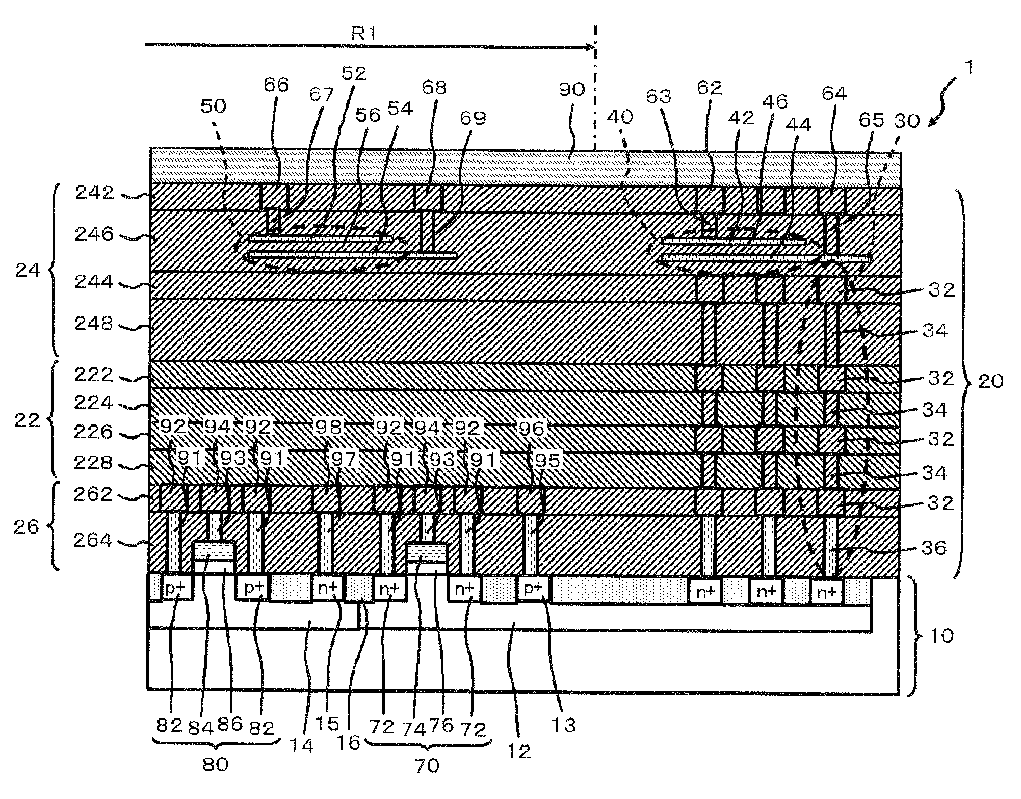
[0018]FIG. 1 is a sectional view showing a semiconductor device 1 of an exemplary embodiment according to the present invention. FIG. 1 illustrates the schematic cross-sectional structure of the semiconductor device 1, similar to that illustrated in FIG. 3. The semiconductor device 1 has a circuit-forming region R1. The semiconductor device 1 further has a semiconductor substrate 10, a plurality of insulating interlayer films 20, a seal ring 30 (or a guard ring), and an MIM capacitor 40 (or a first MIM capacitor). In this embodiment, the semiconductor su...


PUM


Abstract

Disclosed is a semiconductor device which has a circuit-forming region. The semiconductor device has a semiconductor substrate, a plurality of insulating interlayer films, a guard ring, and a first MIM capacitor. The insulating interlayer films, which are stacked one upon another, are provided over the semiconductor substrate. The guard ring is formed in the plurality of insulating interlayer films and surrounds the circuit-forming region. The guard ring is separated from an insulating interlayer film including a topmost interconnect. The MIM capacitor is provided between the guard ring and the insulating interlayer film including the topmost interconnect.

Description

[0001]This application is based on Japanese patent application No. 2007-023508 which is incorporated herein by reference.BACKGROUND[0002]1. Technical Field[0003]The present invention relates to a semiconductor device.[0004]2. Related Art[0005]FIG. 2 is a plan view showing a conventional semiconductor device 100. FIG. 3 is a sectional view taken along line III-III of FIG. 2. In the semiconductor device 100, seal rings 102 are formed so as to surround a circuit-forming region 101, thus preventing penetration of moisture or ions into the circuit-forming region 101. FIGS. 2 and 3 illustrate the exemplary seal rings which have a triple ring structure.[0006]These seal rings 102 are formed, as shown in FIG. 3, in an insulating interlayer structure 111 over a semiconductor substrate 110. Each seal ring 102 extends across the entire thickness of the insulating interlayer structure 111. The insulating interlayer structure 111 is comprised of an insulating interlayer group 111a made of silicon...

Claims


Application Information

Patent Timeline
Patent Type & Authority Applications(United States)
IPC IPC(8): H01L23/552
CPCH01L23/5223H01L23/585H01L2924/0002H01L2924/00
Inventor NAKASHIBA, YASUTAKA
Owner RENESAS ELECTRONICS CORP
Why Eureka
Try Eureka