Formation process of interconnect structures with air-gaps and sidewall spacers

a technology of air gap and sidewall spacer, which is applied in the direction of semiconductor devices, semiconductor/solid-state device details, electrical apparatus, etc., can solve the problems of increasing capacitance coupling between conductors, increasing power consumption, and reducing electro-migration, so as to improve time-dependent dielectric breakdown and reduce electro-migration

Inactive Publication Date: 2008-08-07
TAIWAN SEMICON MFG CO LTD
View PDF13 Cites 49 Cited by
  • Summary
  • Abstract
  • Description
  • Claims
  • Application Information

AI Technical Summary

Benefits of technology

[0013]The advantageous features of the present invention include reduced electro-migration and improved time dependent dielectric breakdown.

Problems solved by technology

In the past, such reductions were limited only by the ability to define the structures photo-lithographically, device geometries having smaller dimensions created new limiting factors.
This increased capacitance results in increased capacitive coupling between the conductors, increased power consumption, and an increase in the resistive-capacitive (RC) time constant.
Furthermore, air-gaps are formed to further reduce effective k value of interconnect structures.
Although the formation of air-gaps 10 reduces the parasitic capacitance of the interconnect structure, the conventional process suffers drawbacks.
Without the back pressure provided by the dielectric layer, electro-migration (EM) is increased, and time dependent dielectric breakdown (TDDB) performance of the interconnect structure is adversely affected.
A further problem is that in subsequent processes for forming overlying vias on the copper lines 4, if misalignment occurs, the vias may land on air-gaps 10, resulting in copper being plated into air-gaps 10.
Without the back pressure provided by the dielectric layer, the EM performance and TDDB performance are adversely affected.
In addition, misalignment of the overlying vias will cause copper to be formed in air-gaps, which will significantly reduce the distances between metal lines, hence an increase in parasitic capacitances.

Method used


Image

  • Formation process of interconnect structures with air-gaps and sidewall spacers
  • Formation process of interconnect structures with air-gaps and sidewall spacers
  • Formation process of interconnect structures with air-gaps and sidewall spacers

Examples


Embodiment Construction

[0020]The making and using of the presently preferred embodiments are discussed in detail below. It should be appreciated, however, that the present invention provides many applicable inventive concepts that can be embodied in a wide variety of specific contexts. The specific embodiments discussed are merely illustrative of specific ways to make and use the invention, and do not limit the scope of the invention.

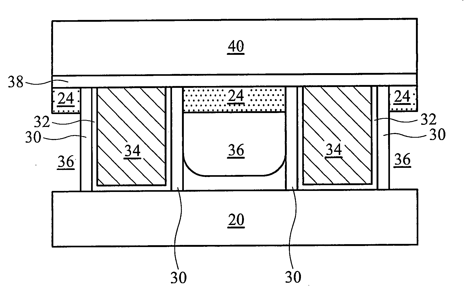
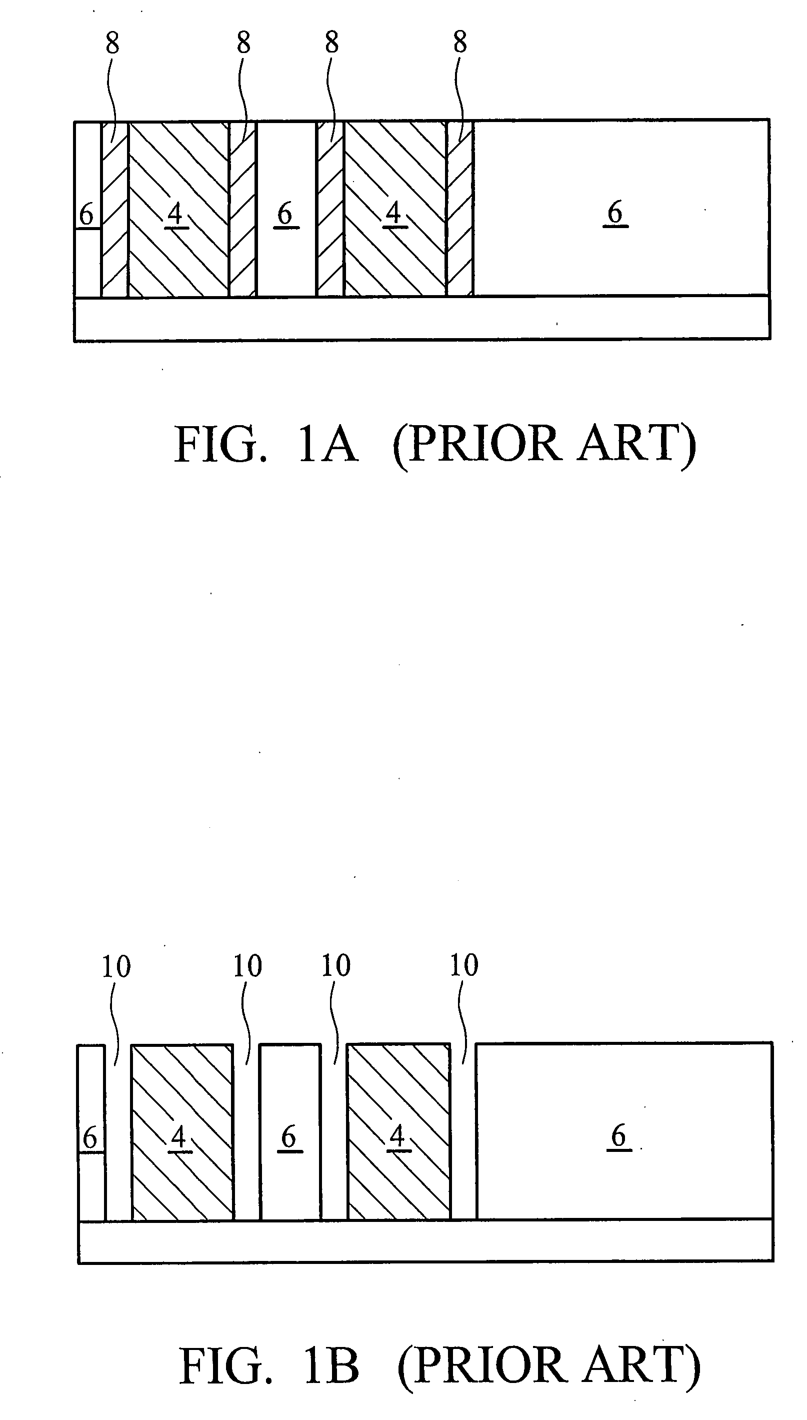
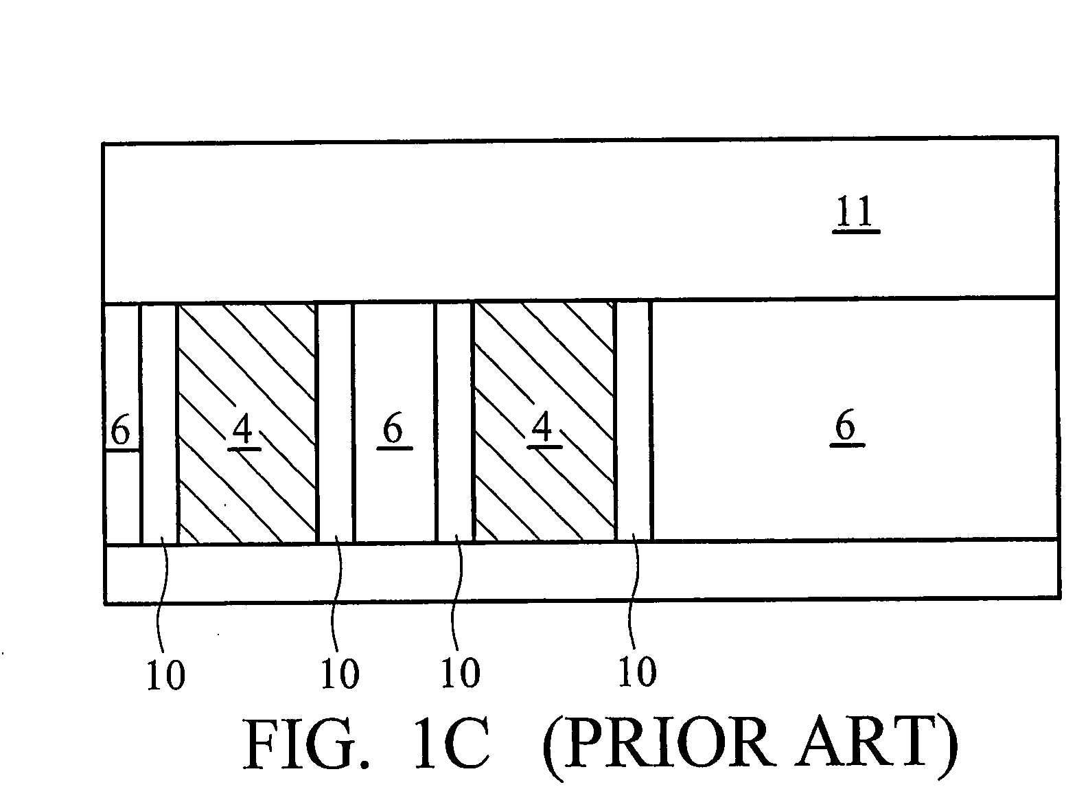
[0021]Interconnect structures with air-gaps and sidewall spacers are provided. The intermediate stages of manufacturing preferred embodiments of the present invention are illustrated. Throughout the various views and illustrative embodiments of the present invention, like reference numbers are used to designate like elements. In the following discussed embodiments, single damascene processes are discussed. One skilled in the art will realize that the teaching is readily available for dual damascene processes.

[0022]FIGS. 4 through 10 are cross-sectional views of intermediate s...


PUM


Abstract

An integrated circuit structure having air gaps is provided. The integrated circuit includes a conductive line; a sidewall spacer on a sidewall of the conductive line, wherein the sidewall spacer comprises a dielectric material; an air-gap horizontally adjoining the sidewall spacer; and a dielectric layer on the air-gap.

Description

TECHNICAL FIELD[0001]This invention relates generally to integrated circuits, and more particularly to structure and formation methods of interconnect structures having air-gaps.BACKGROUND[0002]As the semiconductor industry introduces new generations of integrated circuits (ICs) having higher performance and greater functionality, the density of the elements that form those ICs is increased, while the dimensions, sizes and spacing between components or elements are reduced. In the past, such reductions were limited only by the ability to define the structures photo-lithographically, device geometries having smaller dimensions created new limiting factors. For example, for any two adjacent conductive features, as the distance between the conductive features decreases, the resulting capacitance (a function of the dielectric constant (k value) of the insulating material divided by the distance between the conductive features) increases. This increased capacitance results in increased c...

Claims


Application Information

Patent Timeline
Patent Type & Authority Applications(United States)
IPC IPC(8): H01L23/528
CPCH01L21/7682H01L21/76849H01L21/76831
Inventor LIU, CHUNG-SHIYU, CHEN-HUAMII, YUH-JIERSUN, YUAN-CHEN
Owner TAIWAN SEMICON MFG CO LTD
Why Eureka
Try Eureka