

Wireless system, semiconductor device, and communication device
a communication device and wireless technology, applied in the field of semiconductor devices, can solve the problem that the cost-effective process cannot be used to improve reliability, and achieve the effect of high reliability and high reliability
- Summary
- Abstract
- Description
- Claims
- Application Information
AI Technical Summary
Benefits of technology
Problems solved by technology
Method used
Image

Examples
embodiment mode 1
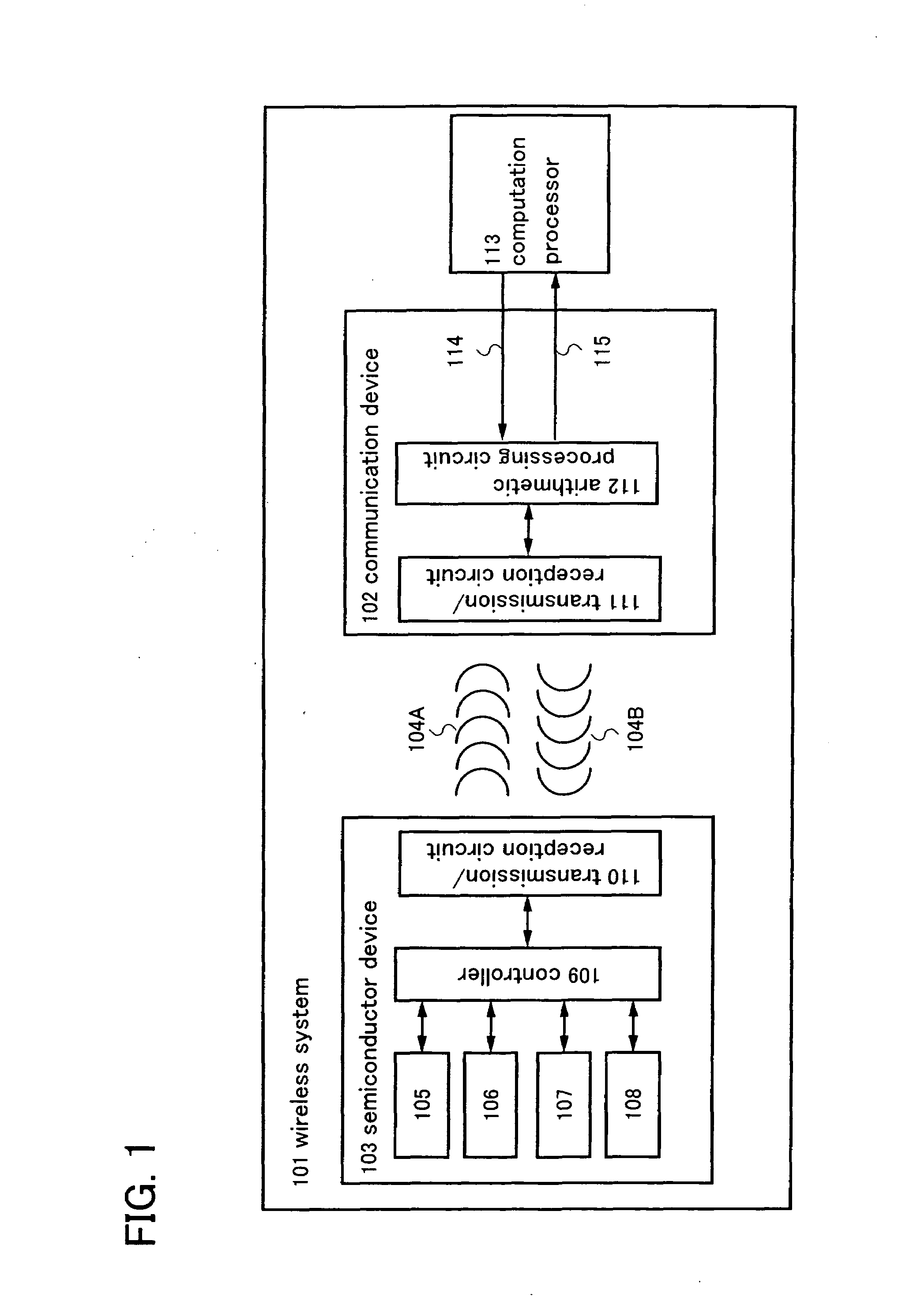
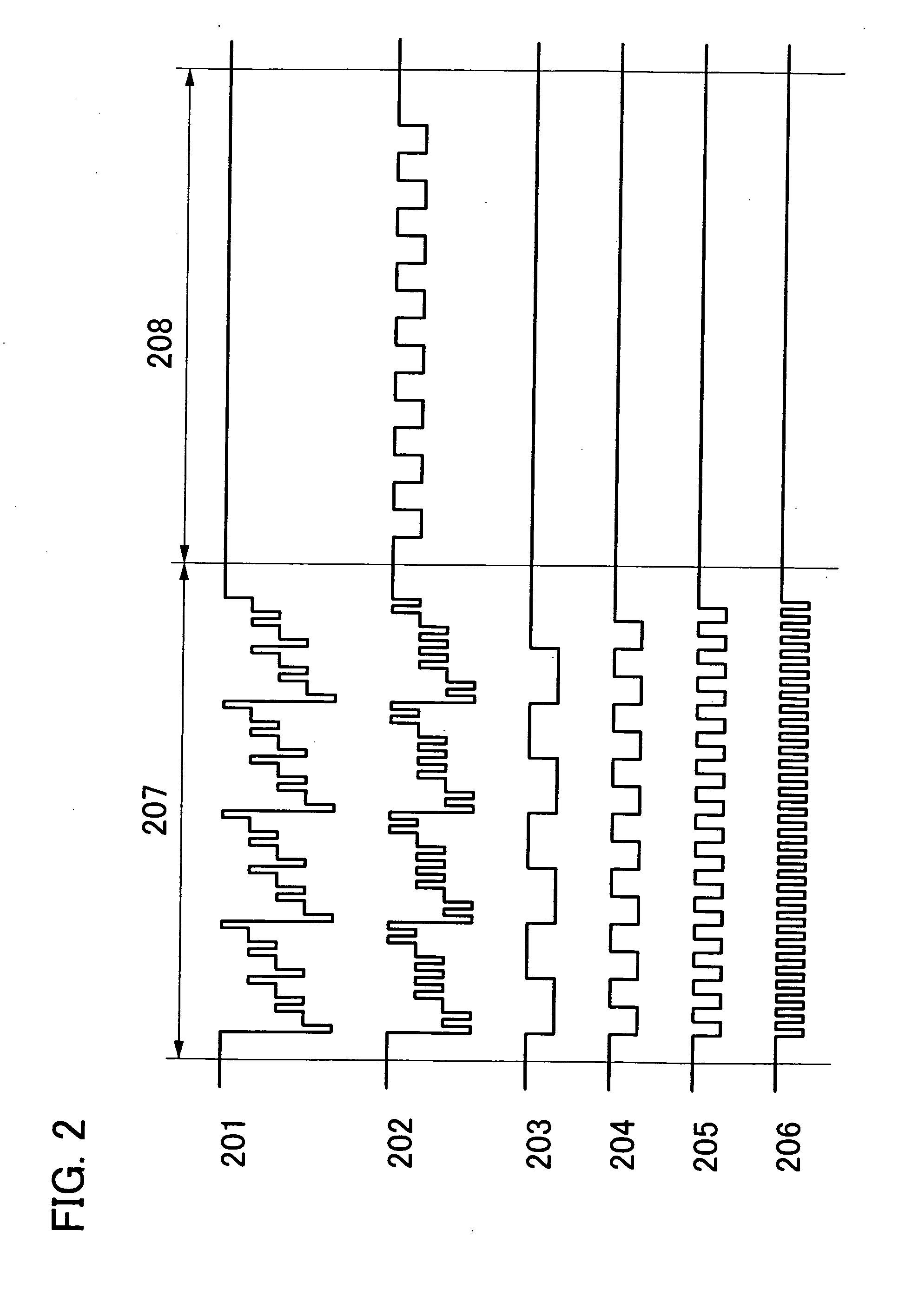
[0031]In this embodiment mode, an exemplary structure of a wireless system in the present invention will be described with reference to FIGS. 1 to 3D. FIG. 1 is a block diagram of the wireless system in the present invention in this embodiment mode. FIG. 2 illustrates radio signals of the wireless system in the present invention in this embodiment mode. FIGS. 3A to 3D illustrate waveforms of radio signals of the wireless system, which are subjected to Fourier transform, in the present invention in this embodiment mode.
[0032]In FIG. 1, a wireless system 101 includes a communication device 102 and a semiconductor device 103. The communication device 102 and the semiconductor device 103 transmit and receive information through a first radio signal 104A and a second radio signal 104B. Note that the first radio signal 104A is a signal from the semiconductor device 103 to the communication device 102, and the second radio signal 104B is from the communication device 102 to the semiconduct...
embodiment mode 2
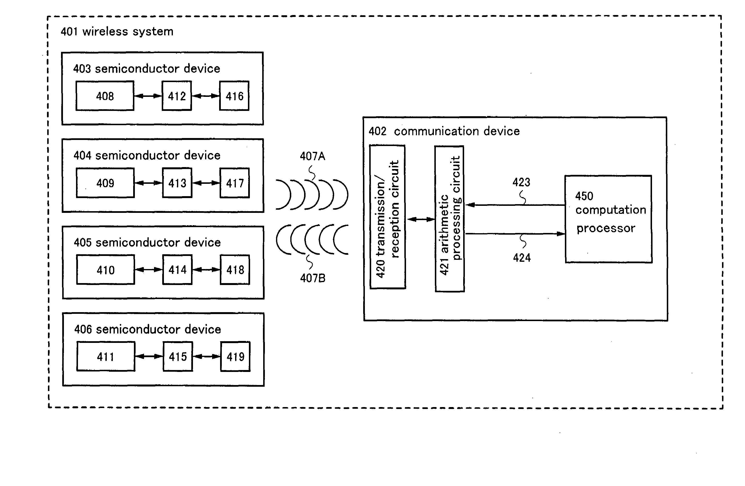
[0063]In this embodiment mode, an exemplary structure of a wireless system, which is different from that described in Embodiment Mode 1, will be described with reference to FIGS. 4 to 6D. FIG. 4 is a block diagram of the wireless system of the present invention in this embodiment mode. FIG. 5 illustrates the waveforms of radio signals in the wireless system of the present invention in this embodiment mode. FIGS. 6A to 6D are Fourier transform waveforms of radio signals in the wireless system of the present invention in this embodiment mode.
[0064]In FIG. 4, a wireless system 401 includes a communication device 402, a first semiconductor device 403, a second semiconductor device 404, a third semiconductor device 405, and a fourth semiconductor device 406. The communication device 402 and the first to fourth semiconductor devices 403 to 406 transmit and receive information through a first radio signal 407A and a second radio signal 407B. Note that the first radio signal 407A is a signa...
embodiment mode 3
[0090]In this embodiment mode, one example of a manufacturing method of the semiconductor device, described in the above embodiment mode, will be described with reference to the drawings. In this embodiment mode, a structure will be described in which a semiconductor device and an antenna circuit are provided over the same substrate. By forming an antenna circuit and a semiconductor device over the same substrate, and using a thin film transistor as a transistor which forms the semiconductor device, a small-size semiconductor device can be provided.
[0091]First, as shown in FIG. 9A, a release layer 1903 is formed over one surface of a substrate 1901 with an insulating film 1902 interposed therebetween, and an insulating film 1904 which functions as a base film, and a semiconductor film 1905 (e.g., a film containing amorphous silicon) are stacked. Note that the insulating film 1902, the release layer 1903, the insulating film 1904, and the semiconductor film 1905 can be sequentially f...
PUM
 Abstract
Description
Claims
Application Information