Display Device and Method of Manufacturing the Same

Inactive Publication Date: 2008-08-14
SAMSUNG ELECTRONICS CO LTD
View PDF3 Cites 13 Cited by
  • Summary
  • Abstract
  • Description
  • Claims
  • Application Information

AI Technical Summary

Benefits of technology

[0014]According to an embodiment of the present invention a display device includes a first conductive layer including a driving source electrode and a driving drain electrode, a second conductive layer insulated from the first conductive layer, and including a driving gate electrode, a switching gate electrode, and a gate line, and a third conductive layer insulated from the first and second conductiv

Problems solved by technology

The thin insulating layer is easily damaged by an operation voltage so that short-circuit between the conductive layers may occur.
The hillock in the conductive layer damages a thin portion of the insulating layer.
Therefore, the hillock in the co

Method used


Image

  • Display Device and Method of Manufacturing the Same
  • Display Device and Method of Manufacturing the Same
  • Display Device and Method of Manufacturing the Same

Examples


Example

[0037]Reference will now be made in detail to embodiments of the present invention, examples of which are illustrated in the accompanying drawings. As those skilled in the art would realize, described embodiments may be modified in various different ways, all without departing from the spirit or scope of the present invention.

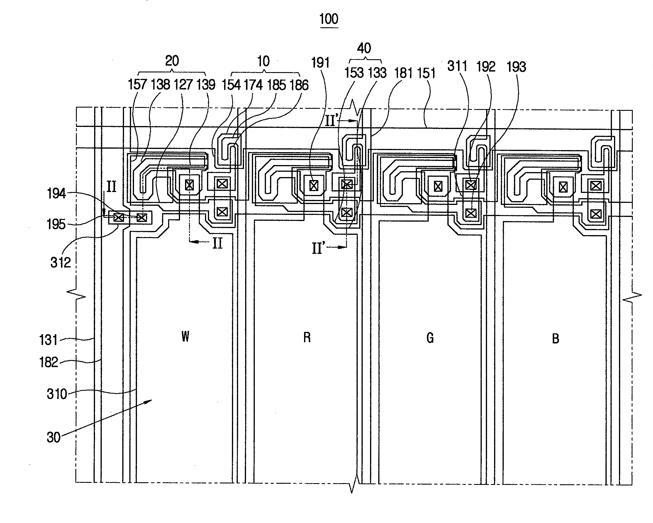
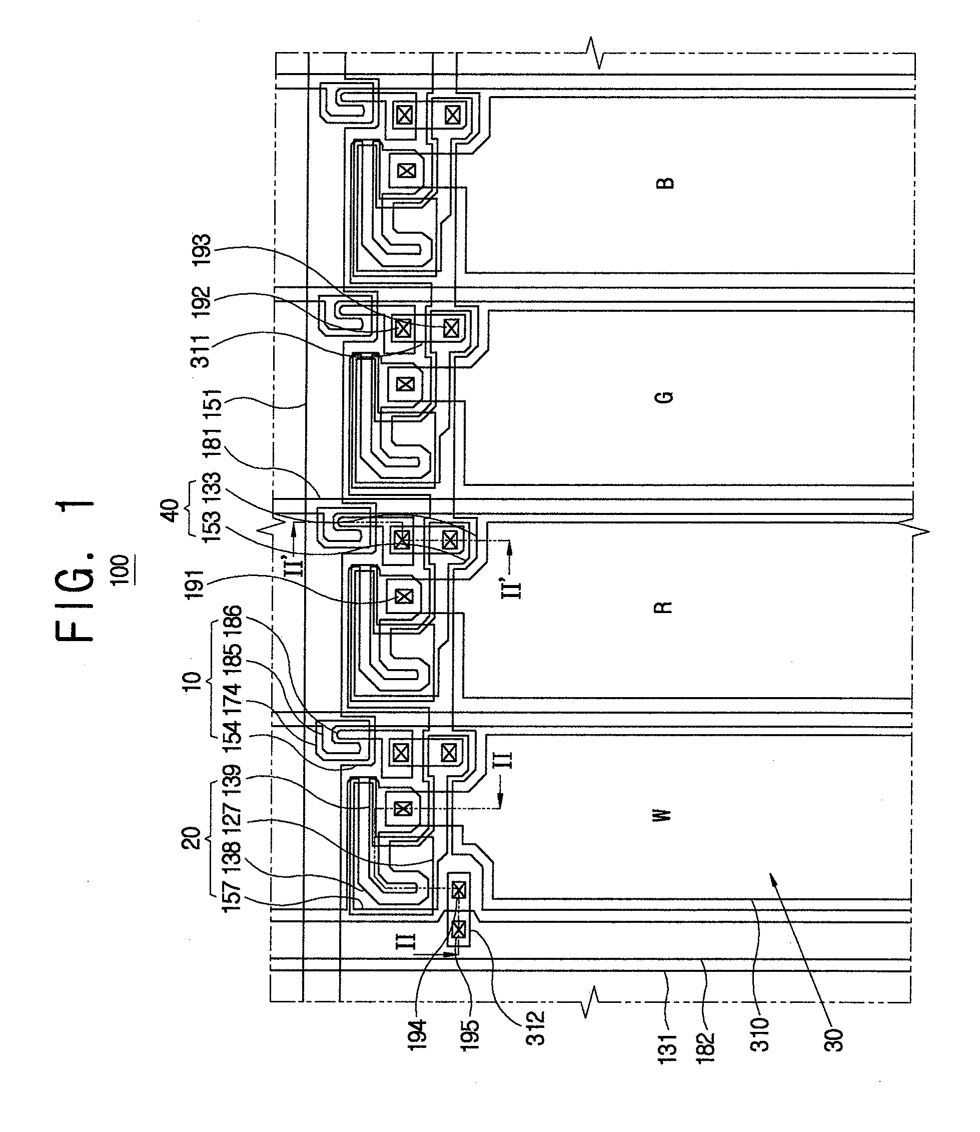
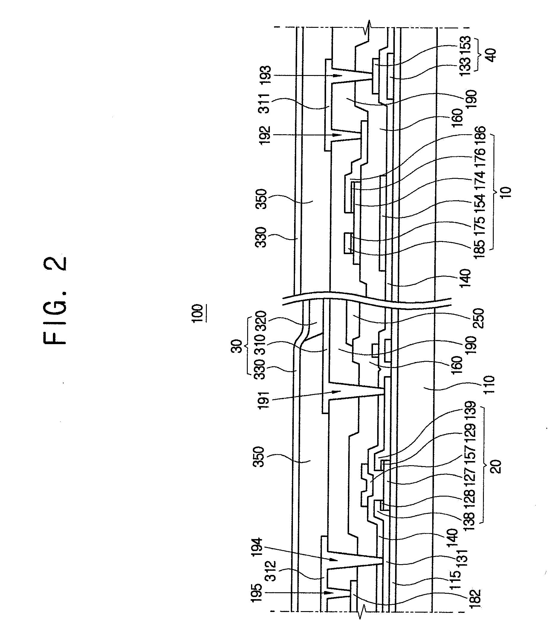
[0038]The accompanying drawings illustrate an organic light emitting diode (OLED) display as a display device.

[0039]In addition, the accompanying drawings illustrate an active matrix (AM)-type OLED display having a 2Tr-1Cap structure wherein one pixel includes two thin film transistors (TFTs) and one capacitor. The structure of the AM-type OLED is not limited thereto.

[0040]The pixel is a minimum unit for display using the display device.

[0041]In the display device, one pixel may include more than three TFTs and more than two capacitors, and additional wiring may be further provided.

[0042]Like reference numerals refer to like elements throughout. Exemplary embod...


PUM


Abstract

A display device includes a first conductive layer including a driving source electrode and a driving drain electrode, a second conductive layer insulated from the first conductive layer, and including a driving gate electrode, a switching gate electrode, and a gate line, and a third conductive layer insulated from the first and second conductive layers, and including a switching source electrode, a switching drain electrode, a data line, and a common power line.

Description

CROSS-REFERENCE TO RELATED APPLICATION[0001]This application claims priority from Korean Patent Application No. 10-2007-0013867, filed on Feb. 09, 2007 in the Korean Intellectual Property Office, the disclosure of which is herein incorporated by reference in its entirety.BACKGROUND OF THE INVENTION[0002]1. Field of the Invention[0003]Apparatuses and methods consistent with the present invention relate to a display device and a manufacturing method thereof, and more particularly, to a display device that suppresses an occurrence of a defect and improves electric characteristics, and a manufacturing method thereof.[0004]2. Discussion of Related Art[0005]There are various types of display devices.[0006]Among the various types of display devices, a liquid crystal display (LCD) device and an organic light emitting diode (OLED) display are light-weighted and small-sized and have performance that improves with developing semiconductor technology.[0007]The LCD device and the OLED display de...

Claims


Application Information

Patent Timeline
IPC IPC(8): H05K1/00H01J1/62H01L21/28H05K1/16H05K1/03H01L51/52
CPCH01L27/1214H01L27/124H01L27/1251H01L27/1255H01L27/12H01L29/458H01L29/4908
Inventor GOH, JOON-CHULYOON, YOUNG-SOO
Owner SAMSUNG ELECTRONICS CO LTD
Why Eureka
Try Eureka