Liquid crystal display
a technology of liquid crystal display and impact resistance, which is applied in the field of liquid crystal display, can solve the problems of insufficient substrate, insufficient impact resistance against the great outer force sufficient for destroying the liquid crystal substrate, and insufficient substrate, etc., and achieves the effect of restricting disturbance of displayed image and sufficient impact resistan
- Summary
- Abstract
- Description
- Claims
- Application Information
AI Technical Summary
Benefits of technology
Problems solved by technology
Method used
Image
Examples
embodiment 2
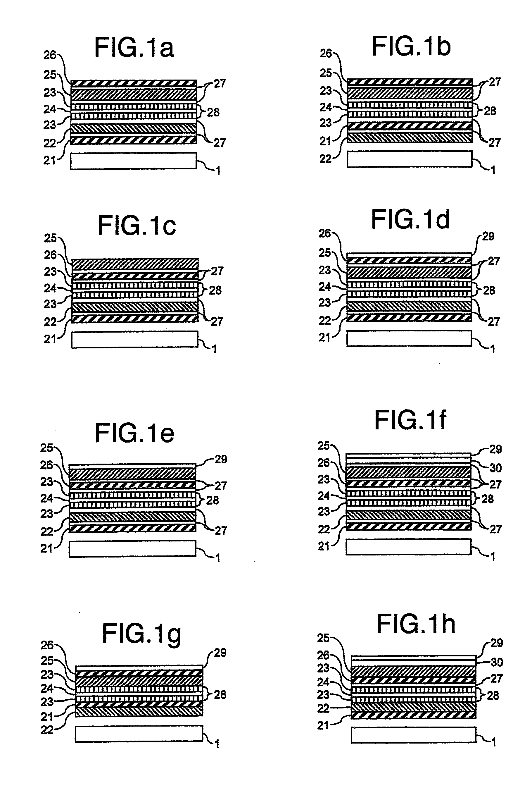
[0035]FIGS. 1d-1f are schematic cross sectional views of embodiments including respective surface treating surfaces 29 closest to the viewer in the panel. Further, in FIG. 1f, a protect film or plate 30 is arranged under the surface treating surface 29 to further increase a physical strength. The protect film or plate 30 may be made of acrylate type resin, polyethylene-terephthalate type resin or the like. It may be a glass plate.
[0036]The surface treating surface 29 may be an anti-reflecting layer, anti-glare layer, anti-fouling layer for preventing fouling from adhering to the surface, or the like. These layers may be stacked. The anti-reflecting layer may be single layer of, for example, SiO2 or MgF2 lower in refractive index than a layer to which the anti-reflecting layer is adhered. Alternatively, the anti-reflecting layer may be multilayer as a stack of high refractive index material, for example, TiO2, ZrO2 or the like and the low refractive index material, for example, SiO2,...
embodiment 3
[0037]FIGS. 1g and 1h are schematic cross sectional views of embodiments including the transparent resin layers 22 and 25 of adhesive, and if adhesion thereof to the polarizing plate or the glass substrate is sufficient, all of the transparent adhesive layers 27 as adhesive for the transparent resin layers 22 and 25 may be eliminated as shown in FIG. 1g, or one of the transparent adhesive layers 27 as adhesive for the transparent resin layers 22 and 25 may be eliminated as shown in FIG. 1h. By eliminating the transparent adhesive layer 27, the thickness of the panel is decreased, and a producing process of the panel is simplified. In FIGS. 1g and 1h, the polarizing plate may be adhered to the transparent resin layer after the transparent resin layer is adhered to the glass plate. In these embodiments, the polarizing plate with the transparent resin layer or the polarizing plate with the wavelength plate may be used, and these layers may be stacked through the adhesive.
[0038]Hereafte...
PUM
| Property | Measurement | Unit |
|---|---|---|
| thickness | aaaaa | aaaaa |
| thickness | aaaaa | aaaaa |
| thickness | aaaaa | aaaaa |
Abstract
Description
Claims
Application Information
 - R&D
- Intellectual Property
- Life Sciences
- Materials
- Tech Scout
- Unparalleled Data Quality
- Higher Quality Content
- 60% Fewer Hallucinations
Browse by: Latest US Patents, China's latest patents, Technical Efficacy Thesaurus, Application Domain, Technology Topic, Popular Technical Reports.
© 2025 PatSnap. All rights reserved.Legal|Privacy policy|Modern Slavery Act Transparency Statement|Sitemap|About US| Contact US: help@patsnap.com


