Semiconductor charge multiplication amplifier device and semiconductor image sensor provided with such an amplifier device

a multi-amplifier and semiconductor technology, applied in the field of semiconductor image sensor provided with such an amplifier device, can solve the problems of recited prior art deficient in providing linear amplification, various drawbacks associated with prior art technology, etc., and achieve the effect of reducing the above modulating effect and raising the operational stability of the device further

Active Publication Date: 2008-08-14
TELEDYNE DIGITAL IMAGING INC
View PDF5 Cites 8 Cited by
  • Summary
  • Abstract
  • Description
  • Claims
  • Application Information

AI Technical Summary

Benefits of technology

[0005]Now therefore, according to one of its aspects, the invention is characterized in that it comprises a charge-biasing facility below which as viewed in projection the impact ionization facility is formed in the semiconductor body, which is positioned as viewed in projection between two neighboring clock electrodes and which is arranged for being driven at a first substantially static electric potential (DC2) for controlling the electric field strength in the impact ionization facility. Especially, the static control of the output side of the amplification allows for mitigating the above modulating effects.
[0006]Advantageously, the impact ionization facility is arranged for being driven at a second substantially static electric potential (DC1) for collectively with said first substantially static electric potential (DC2) controlling the electric field strength in the impact ionization facility. Now, the difference between two static voltages will completely and precisely control the electric field strength in the impact ionization region.
[0007]Advantageously, an electrode for applying said first substantially static electric potential (DC2) is followed by at least one output electrode that is arranged for being driven by at least one first dynamic electric potential (30, 32) for removing charge carriers away from said impact ionization facility. This raises the operational stability of the device still further by resorting to stable and straightforward DC potentials.
[0008]Advantageously, such device stage is arranged in a multi-stage amplification facility, wherein successive impact ionization facilities are separated by a sequence of at least a first and a second pulsed control electrode, that are driven by a first and a second dynamic partial electric potential, respectively, wherein said first and second partial potentials are overlapping for collectively bringing charge carriers from the first static electric potential (DC2) of a preceding stage to the second static electric potential (DC1) of a next succeeding stage. Combined with earlier advantageous features, this arrangement will diminish the necessary amplitudes of the pulsed control voltages.

Problems solved by technology

However, various drawbacks are associated to the prior art technology.
Secondly, and even more pertinent, the recited prior art is deficient in providing a linear amplification, because the charge multiplication in an output register strongly depends on the effective potential difference under adjacent gates in a multiplication stage.

Method used


Image

  • Semiconductor charge multiplication amplifier device and semiconductor image sensor provided with such an amplifier device
  • Semiconductor charge multiplication amplifier device and semiconductor image sensor provided with such an amplifier device
  • Semiconductor charge multiplication amplifier device and semiconductor image sensor provided with such an amplifier device

Examples


Embodiment Construction

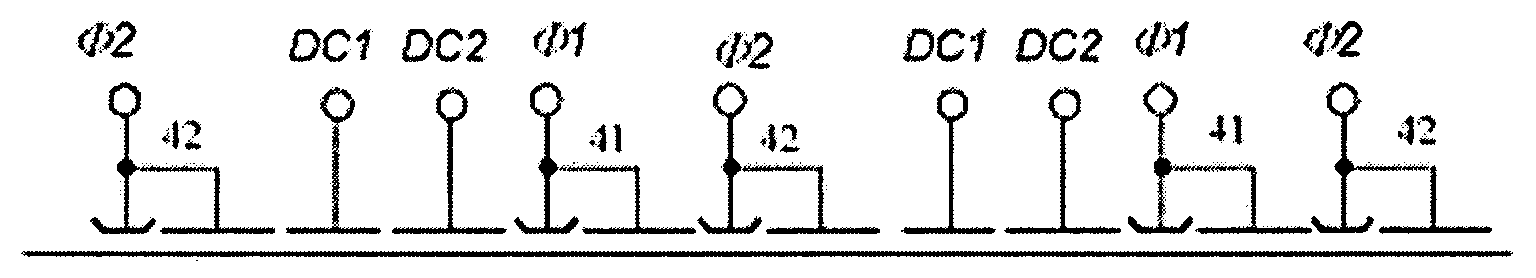
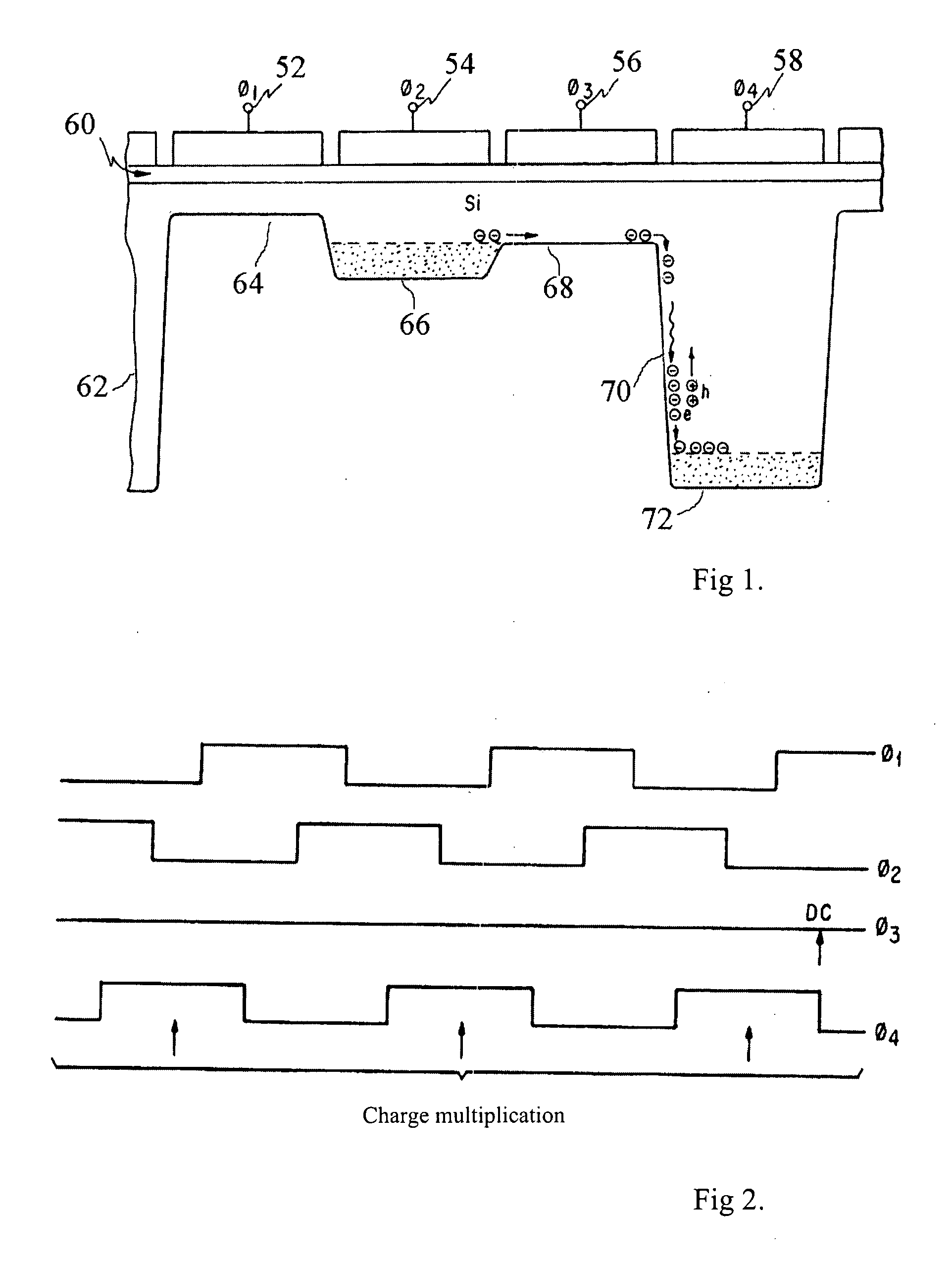
[0020]First, for better understanding of the invention, a device according to the prior art will be briefly presented. In this respect, FIG. 1 illustrates a comprehensive cross-sectional view 50 of such prior art device together with associated controls. First, a solid-state circuitry representation is shown at the top of the Figure. As shown, a repetitive pattern of electrodes 52 through 58 is present from left to right, each electrode of a group of four adjacent electrodes having its own clock pulse sequence numbered from Φ1 to Φ4. As shown, the electrodes are disposed on a silicon gate oxide layer 60 that itself sits on p-type silicon substrate 62. For brevity, driving electronics and input / output facilities have been omitted. The present invention lends itself to various alternative implementations such as n-type silicon, which alternatives will furthermore not be specifically discussed for brevity.

[0021]As furthermore shown, a potential curve for the channel from left to right ...


PUM


Abstract

A charge multiplication amplifier device comprises a series arrangement of a first separation barrier facility, a temporary storage well for charge carriers, a second charge transfer barrier facility, an impact ionization facility that is operative through electric field strength effective on mobile charge carriers, and a charge collection well for receiving charge carriers so multiplied.Advantageously, the device comprises a charge collection and transfer facility (32) that is geometrically disposed next to the impact ionization facility (31) whereas impact ionization facility is controlled at a substantially static electric potential (DC1, DC2) for controlling the electric field strength.Advantageously, another embodiment of this device comprises charge collection and transfer facilities (41, 42) implemented as two (or more) independently clocked signals Φ1, Φ2 that require nearly two times less swing to achieve same effect.

Description

BACKGROUND OF THE INVENTION[0001]The invention relates to a semiconductor charge multiplication amplifier device stage that comprises a series arrangement of a plurality of clock electrodes (81,82) on top of a semiconductor body for transporting through the semiconductor body packages of charge carriers from an image sensor section towards an output section, the device further comprising an impact ionization facility for by means of applying an electric field strength multiplying the charge carriers during their transport from the image section to the output section,[0002]Prior art, as represented by U.S. Pat. No. 5,337,340 to Jaroslav Hynecek and assigned to Texas Instruments of Dallas, Tex., has recognized advantageous properties of charge multiplication devices which are operative through ionizing field strengths, or colloquially called “avalanche devices” that are especially, but not exclusively, intended for use in image sensor devices based on CCD technology. This technology a...

Claims


Application Information

Patent Timeline
Patent Type & Authority Applications(United States)
IPC IPC(8): G11C19/28
CPCH01L27/1485
Inventor LAZOVSKY, LEONID YURIEVICH
Owner TELEDYNE DIGITAL IMAGING INC
Why Eureka
Try Eureka