Nanotip capacitor

a capacitor and nanotip technology, applied in the direction of capacitors, transistors, semiconductor devices, etc., can solve the problems of incompatibility of the fabrication process with the conventional silicon (si) integrated circuit (ic) process, difficult to efficiently fabricate electrical devices from nanowires, and fragile metal nanowires, etc., to achieve the effect of ultra-large capacitan

Inactive Publication Date: 2008-08-21
SHARP KK
View PDF7 Cites 31 Cited by
  • Summary
  • Abstract
  • Description
  • Claims
  • Application Information

AI Technical Summary

Benefits of technology

[0008]The present invention describes an electronic solid state capacitor which has an ultra-large capacitance per u

Problems solved by technology

However, metallic nanowires are fragile, and it is difficult to efficiently fabricate electrical devices from nanowires.
Arogel-based supercapacitors have very large energy storage capa

Method used


Image

  • Nanotip capacitor
  • Nanotip capacitor
  • Nanotip capacitor

Examples


Embodiment Construction

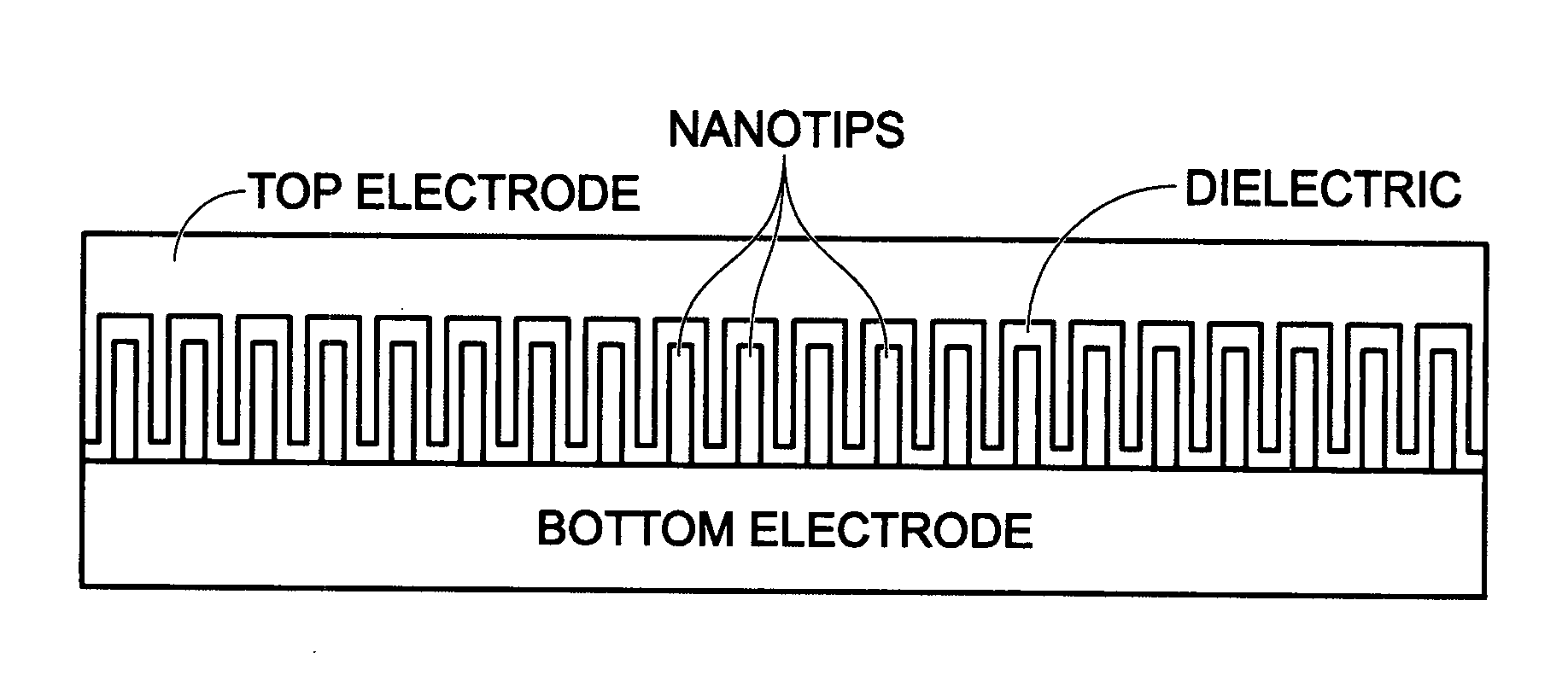
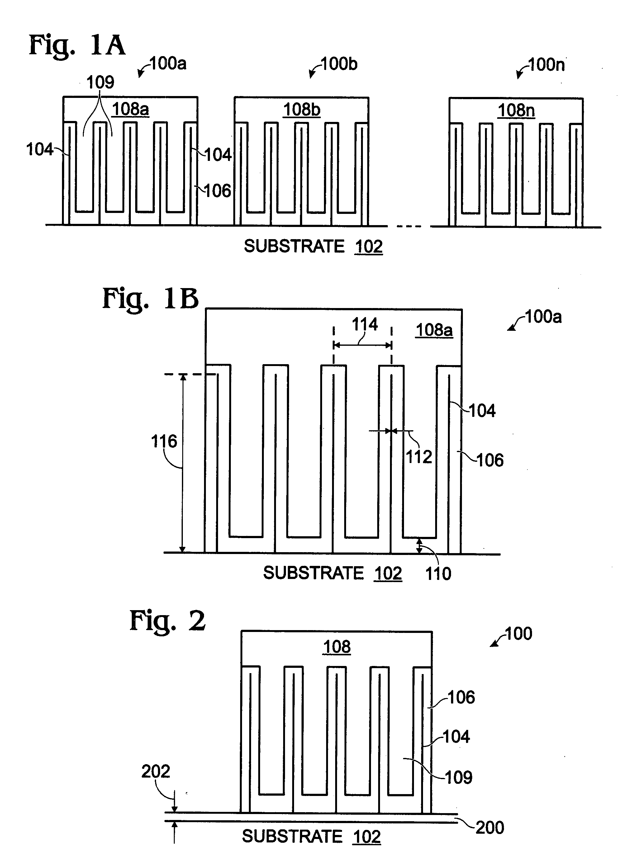
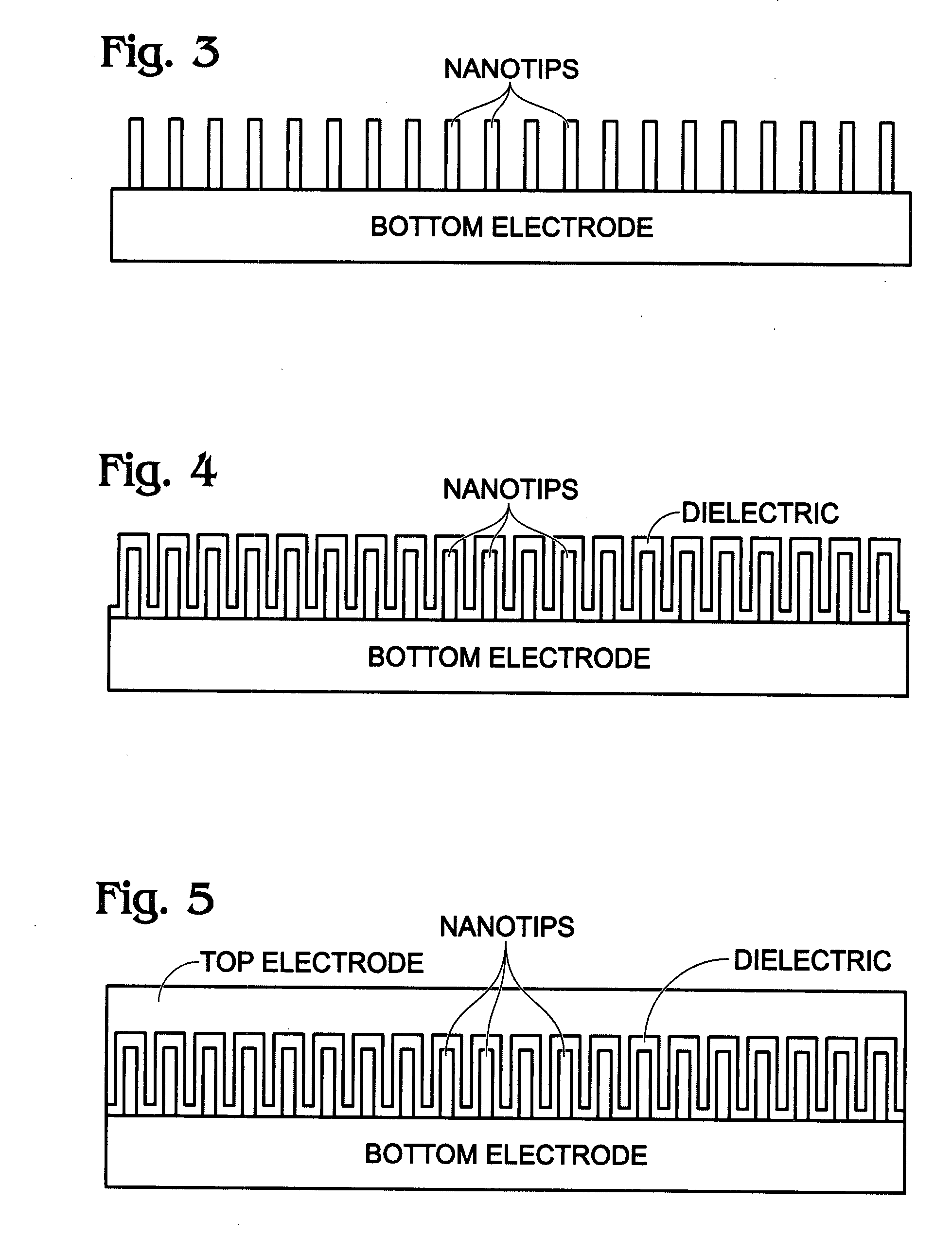
[0018]FIGS. 1A and 1B are partial cross-sectional views of a nanotip capacitor. As seen in FIG. 1A, the nanotip capacitor 100 comprises a bottom electrode 102, with electrically conductive nanotips 104 overlying the bottom electrode 102. Alternately, a nanotip 104 may be referred to as a nanorod, nanostructure, nanowire, or nanotube. An electrically insulating dielectric 106 covers the nanotips 104. An electrically conductive top electrode 108 overlies dielectric-covered nanotips 104. Typically, a plurality of isolated nanotip capacitors 110a, 100b, and 100n are formed with isolated top electrodes, 108a, 108b, and 108n, respectively. Although only three capacitors are depicted, the capacitor array is not limited to any particular number. All the nanotips 104 are connected to a common bottom electrode 102. Although shown as part of a capacitor array, the capacitor 100 may be formed as a single discrete element (see FIGS. 2 and 1B).

[0019]More explicitly, the dielectric-covered nanotip...


PUM


Abstract

A nanotip capacitor and associated fabrication method are provided. The method provides a bottom electrode and grows electrically conductive nanotips overlying the bottom electrode. An electrically insulating dielectric is deposited overlying the nanotips, and an electrically conductive top electrode is deposited overlying dielectric-covered nanotips. Typically, the dielectric is deposited by forming a thin layer of dielectric overlying the nanotips using an atomic layer deposition (ALD) process. In one aspect, the electrically insulating dielectric covering the nanotips forms a three-dimensional interface of dielectric-covered nanotips. Then, the electrically conductive top electrode overlying the dielectric-covered nanotips forms a three-dimensional top electrode interface, matching the first three-dimensional interface of the dielectric-covered nanotips.

Description

BACKGROUND OF THE INVENTION[0001]1. Field of the Invention[0002]This invention generally relates to integrated circuit (IC) fabrication and, more particularly, to a nanotip capacitor and a method for fabricating the same.[0003]2. Description of the Related Art[0004]Recently, the fabrication of nanowires has been explored, due to its potential importance as a building block in nano, microelectromechanical (MEM), and nanoelectromechanical NEM device applications. For example, researchers associated with Charles Lieber of Harvard University have reported the synthesis of a variety of semiconductor nanowires made from materials such as silicon (Si), Si-germanium (SiGe), InP, and GaN, for use in building nano-computing system. Other groups have also reported using templates structures to grow metallic nanowires made of materials such as Ni, NiSi, Au, and Pt. Metallic nanowires can be used as interconnections and the sharp tips of the nanowire make them effective for field emission purpos...

Claims


Application Information

Patent Timeline
IPC IPC(8): H01L29/94H01L21/02
CPCB82Y10/00H01L29/94H01L29/66083H01L28/91
Inventor HSU, SHENG TENGZHANG, FENGYAN
Owner SHARP KK
Why Eureka
Try Eureka