Semiconductor device having at least two layers of wirings stacked therein and method of manufacturing the same

a technology of semiconductor devices and wirings, which is applied in the direction of semiconductor devices, semiconductor/solid-state device details, electrical apparatus, etc., can solve the problems that the reliability of cu wirings has become more important and difficult than ever, and achieve the effect of small variations in initial via resistance values and high reliability

Inactive Publication Date: 2008-08-21
RENESAS ELECTRONICS CORP
View PDF6 Cites 7 Cited by
  • Summary
  • Abstract
  • Description
  • Claims
  • Application Information

AI Technical Summary

Benefits of technology

[0015]According to the above-described embodiments of the present invention, it is possible to provide a semiconductor devi

Problems solved by technology

With the above-described changes in wiring material and method of forming a wiring, a new type of problem referred to as an SIV (Stress Induced Voiding, the same applies to the following) arises in addition to

Method used


Image

  • Semiconductor device having at least two layers of wirings stacked therein and method of manufacturing the same
  • Semiconductor device having at least two layers of wirings stacked therein and method of manufacturing the same
  • Semiconductor device having at least two layers of wirings stacked therein and method of manufacturing the same

Examples


first embodiment

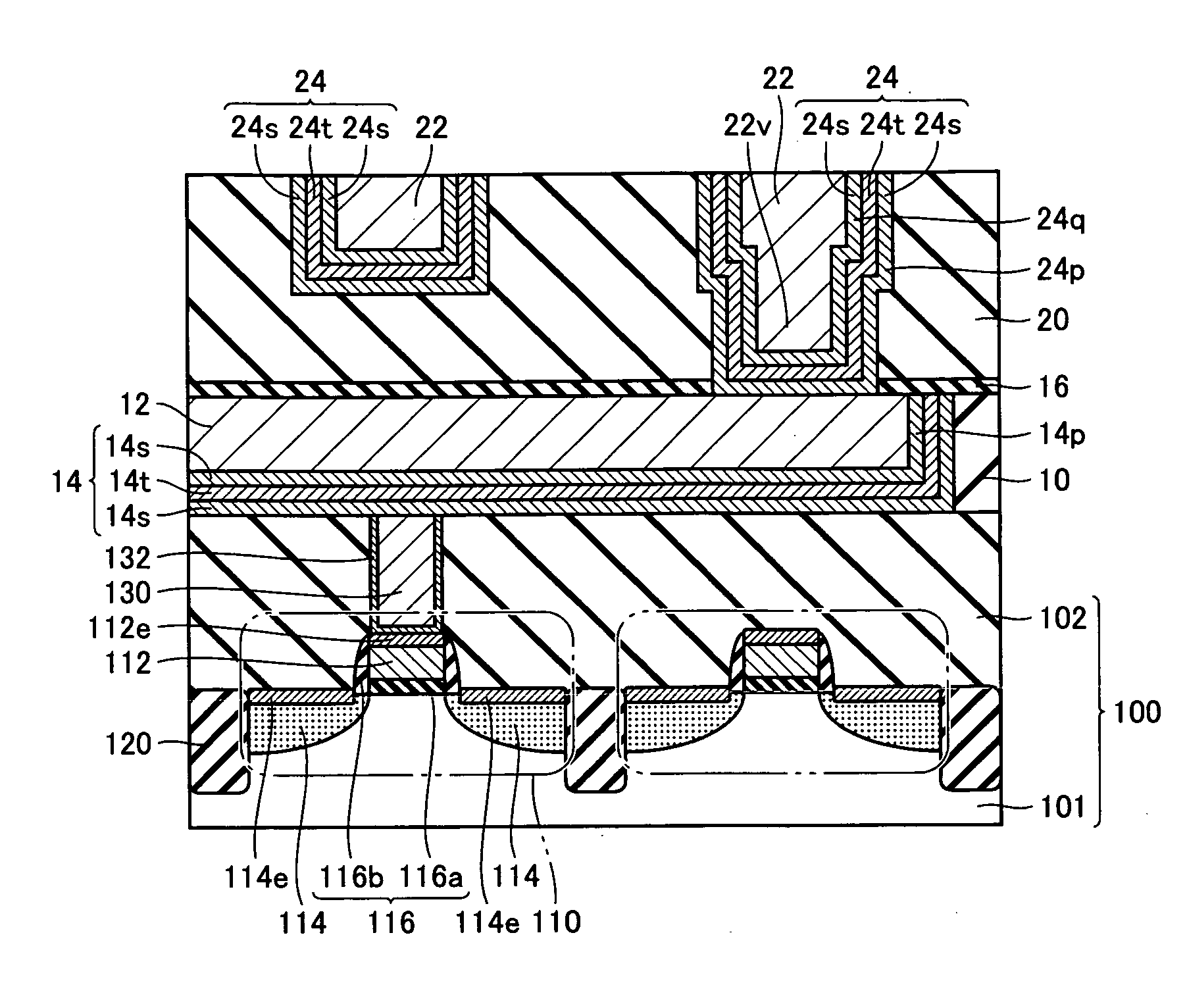
[0042]With reference to FIG. 1, an embodiment of a semiconductor device according to the present invention is a semiconductor device having a first wiring 12 formed in a first insulating layer 10 and a second wiring 22 formed in a second insulating layer 20 formed on first insulating layer 10 and first wiring 12. Here, at least one of first wiring 12 and second wiring 22 is a CuAl wiring formed of a CuAl alloy. Second wiring 22 is electrically connected to first wiring 12 at its via-plug portion 22v, with a plurality of barrier layers 24 interposed therebetween. In the plurality of barrier layers 24, a CuAl-contact barrier layer which is in contact with the CuAl wiring has a nitrogen atom content of less than 10 atomic %, and preferably less than 1 atomic %. Here, it is preferable that a barrier layer 24s mainly contains metal atoms from a viewpoint of reducing electrical resistance between the wirings, and specifically has a metal atom content of at least 90 atomic %.

[0043]In the p...

second embodiment

[0061]With reference to FIG. 7, another embodiment of the semiconductor device according to the present invention is a semiconductor device which has first wiring 12 formed in first insulating layer 10, and second wiring 22 formed in second insulating layer 20 formed on first insulating layer 10 and first wiring 12. Here, at least one of first wiring 12 and second wiring 22 is a CuAl wiring formed of a CuAl alloy. Second wiring 22 is electrically connected to first wiring 12 at its via-plug portion 22v with the plurality of barrier layers 24 interposed therebetween. In the plurality of barrier layers 24, a CuAl-contact barrier layer which is in contact with the CuAl wiring has a nitrogen atom content of less than 10 atomic %, and preferably less than 1 atomic %. Here, the semiconductor device according to the present embodiment is characterized in that first barrier layer 24p which is in contact with first wiring 12 is selectively formed directly below via-plug portion 22v of second...

third embodiment

[0081]With reference to FIG. 14, still another embodiment of the semiconductor device according to the present invention is a semiconductor device having first wiring 12 formed in first insulating layer 10, and second wiring 22 formed in second insulating layer 20 formed on first insulating layer 10 and first wiring 12. Here, at least one of first wiring 12 and second wiring 22 is a CuAl wiring formed of a CuAl alloy. Second wiring 22 is electrically connected to first wiring 12 at is via-plug portion 22v with the plurality of barrier layers 24 formed of a metal interposed therebetween. In the plurality of barrier layers 24, a CuAl-contact barrier layer which is in contact with the CuAl wiring has a nitrogen atom content of less than 10 atomic %, and preferably less than 1 atomic %. Here, the semiconductor device according to the present embodiment is characterized in that first barrier layer 24p which is in contact with first wiring 12 is selectively formed directly on first wiring...


PUM


Abstract

A semiconductor device according to the present invention is a semiconductor device having a first wiring formed in a first insulating layer and a second wiring formed in a second insulating layer formed on the first insulating layer and the first wiring. Here, at least one of the first wiring and the second wiring is a CuAl wiring. The second wiring is electrically connected to the first wiring at its via-plug portion, with a plurality of barrier layers interposed between the second wiring and the first wiring. In the barrier layers, a CuAl-contact barrier layer which is in contact with the CuAl wiring has a nitrogen atom content of less than 10 atomic %. Therefore, the present semiconductor device has high reliability and small variations in initial via resistance value.

Description

BACKGROUND OF THE INVENTION[0001]1. Field of the Invention[0002]The present invention relates to a semiconductor device having at least two layers of wirings stacked therein and a method of manufacturing the same. Specifically, the present invention relates to a semiconductor device having a first wiring formed in a first insulating layer and a second wiring formed in a second insulating layer formed on the first insulating layer and the first wiring, and a method of manufacturing the same.[0003]2. Description of the Background Art[0004]After the development of wirings in the 130 nm node generation, copper has widely been used as a wiring material in semiconductor devices instead of an aluminum-based alloy (which refers to an alloy having a composition of aluminum of at least 50 atomic %, the same applies to the following), for the purpose of reducing resistance of the wiring. Consequently, as a method of forming a wiring, a so-called dual damascene method has been used instead of a...

Claims


Application Information

Patent Timeline
IPC IPC(8): H01L23/52H01L21/4763
CPCH01L21/76843H01L21/76846H01L21/76849H01L21/76864H01L21/76873H01L2924/0002H01L23/53233H01L23/53238H01L2924/00
Inventor MORI, KENICHIMAEKAWA, KAZUYOSHIAMO, NORIAKI
Owner RENESAS ELECTRONICS CORP
Why Eureka
Try Eureka