Stacked Package and Method of Fabricating the Same

a technology of stacked packages and manufacturing methods, applied in the direction of semiconductor devices, semiconductor/solid-state device details, electrical devices, etc., can solve the problems of increasing manufacturing costs, increasing costs, and embracing reliability problems of stacked packages, so as to reduce the height of stacked packages, shorten the signal length, and facilitate fabrication and visual inspection

Inactive Publication Date: 2008-08-28
UNISEMICON
View PDF85 Cites 11 Cited by
  • Summary
  • Abstract
  • Description
  • Claims
  • Application Information

AI Technical Summary

Benefits of technology

[0040]As described above, according to the present invention, the height of a stacked package can be reduced and simultaneously shorten the signal length between BGA packages, thereby enabling the fabrication of high-speed stacked packages.
[0041]Furthermore, in the stacked package of the invention, a soldering can be carried out from outside, thereby enabling an easy fabrication and visual inspection, and also a mass production, which leads to reduction in the manufacturing cost.

Problems solved by technology

However, this stacked package embraces a problem in its reliability, which is caused by the joining between the first and second packages 10A and 10B and the polyimide film 12.
In addition, since the polyimide film 12 is assembled in two pieces, the assembling and treatment process is complicated to thereby increase the manufacturing cost thereof.
However, this stacked package has problems in that the first, second, third PCBs 22A, 22B, 22C cause an additional cost and the entire height of the package increases.
Furthermore, the third PCB 22C is to be further installed beside the first and second PCBs 22A, 22B, and thus the size of the resultant stacked package increases disadvantageously.
Furthermore, the second BGA package causes a trouble in heat-dissipating, thereby failing to apply to a stacked package for high speed.

Method used


Image

  • Stacked Package and Method of Fabricating the Same
  • Stacked Package and Method of Fabricating the Same
  • Stacked Package and Method of Fabricating the Same

Examples


first embodiment

[0077]FIG. 4 is a cross-section illustrating a stacked package according to the invention.

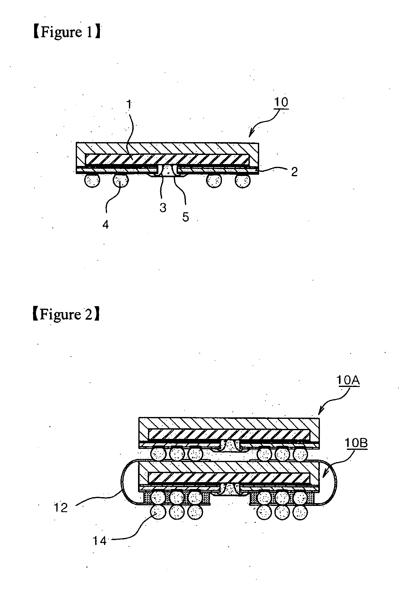
[0078]As shown in FIG. 4, the stacked package of the first embodiment is provided with a circuit board 110 having a circuit pattern for electrically connecting signals. On the top surface of the circuit board 110 is surface-mounted a first ball grid array (BGA) package 120 so as to enable to connect electrical signals, and at the bottom surface of the circuit board 120 is laminated a second BGA package 130 by using an adhesive.

[0079]The second BGA package 120 is provided with a signal connection pad 132 formed so as to be exposed when fabricating the second BGA package 130.

[0080]The signal connection pad 132 and the circuit pattern provided in the circuit board 110 are electrically connected by means Of a signal connection member 140. This signal connection member 140 may be formed of a lead wire, for example, a gold wire. In order to protect the gold wire, preferably, the bonding area of the g...

second embodiment

[0091]FIG. 12 is a cross-section showing a stacked package according to the invention.

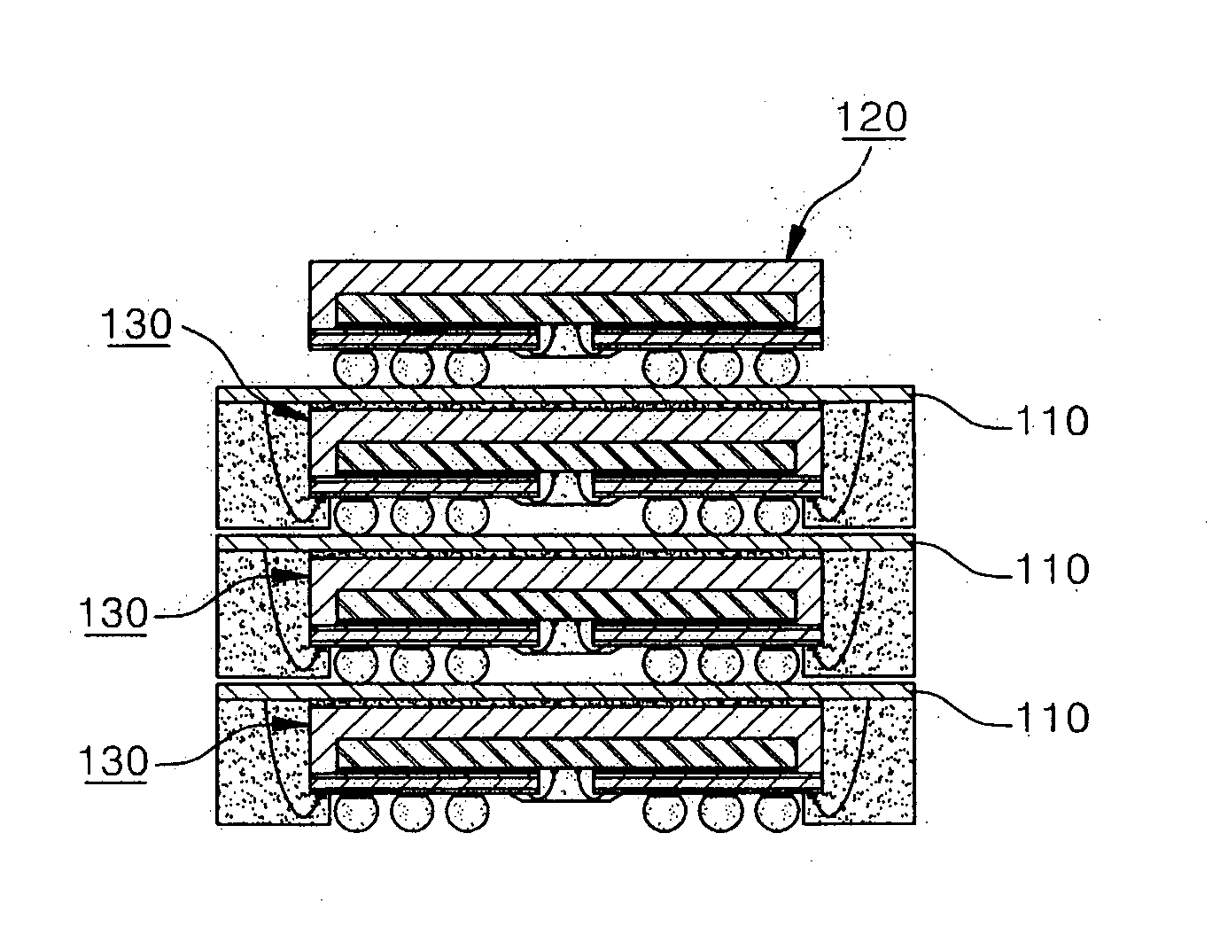
[0092]Referring to FIG. 12, in the stacked package of the second embodiment, the circuit board 110 and the second BGA package 130 attached at the bottom surface thereof are stacked in multiple layers and electrically connected by a surface mounting technique. Similarly, the circuit board 110 and the second BGA package 130 in each layer are electrically signal-connected by a gold wire bonding. That is, the first BGA package 120 of the first embodiment is mounted singularly, and the second BGA package and the circuit board 110 are laminated in multiple layers.

[0093]The manufacturing process of the stacked package of second embodiment will be described. In the first embodiment, the processes of FIGS. 5 to 10 are repeated and then the resultant plural products are stacked in a multi-layered form using a surface mounting so as to be electrically connected with one another. Thereafter, the process of FIG...

third embodiment

[0094]FIG. 13 is a cross-section of a stacked package according to the invention.

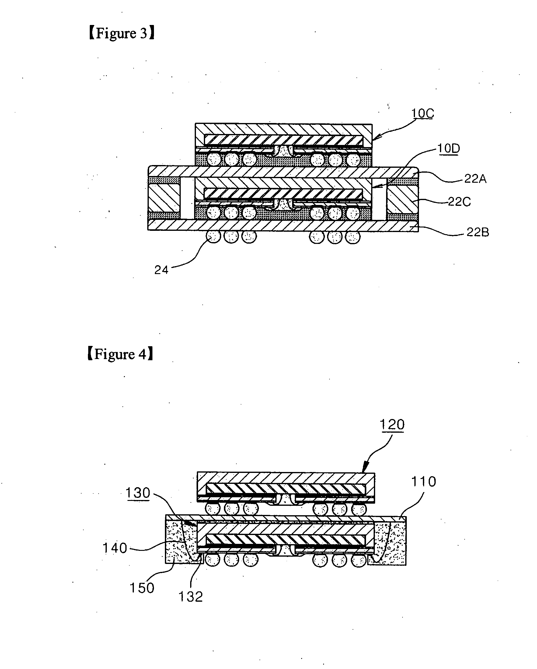
[0095]As shown in FIG. 13, the stacked package of the third embodiment is provided with a first circuit board 210A formed so as to enable to connect electrical signals. On the top surface of the first circuit board 210A is mounted a first BGA package 220A through a surface mounting so as to be electrically connected, and on the bottom surface of the first circuit board 210A is attached a second BGA package 220B.

[0096]On the bottom surface of the second BGA package 220B is surface-mounted a second circuit board 210B so as to be electrically signal-connected. The first circuit board 210A and the second circuit board 210B are made to be electrically signal-connected through a signal connection member 240, which may be a gold wire.

[0097]In addition, an insulation material 250 such as a resin material encloses the bonding area of the gold wire to thereby protect the gold wire. On the bottom face of the secon...


PUM


Abstract

Disclosed herein is a stacked package. The stacked package includes two or more of a first BGA package and a second BGA package and a circuit board having a circuit pattern. The first BGA package is mounted on one face of the circuit board, and the second BGA package is mounted on the other face of the circuit board. A signal connection member is provided for transmitting signals of the first BGA package and the second BGA package to each other. The second BGA package is provided with a signal connection pad. One end of the signal connection member is bonded to the signal connection pad and the other end of the signal connection member is bonded to the circuit pattern of the circuit board. A method of fabricating the stacked package is also disclosed.

Description

FIELD OF THE INVENTION[0001]The present invention relates to a stacked package and a method of fabricating the same. In particular, the invention relates to a stacked package and a fabricating method thereof using a fine-pitch ball grad array semiconductor package (hereinafter, referred to as a “BGA package”), in which the signal length can be shortened and the height thereof can be minimized, thereby providing a high-speed stacked package and enabling a mass production therefor.BACKGROUND OF THE INVENTION[0002]In general, a semiconductor element and a packaging technology therefor are closely related, and thus ceaseless attempts and efforts have been made in order to achieve a high-density, high-speed, miniaturized thin package. In particular, as the package structure has been changed into a surface-mounting mode from the pin-inserting mode, the mounting density of a circuit board has been dramatically improved.[0003]Recently, a chip scale package (CSP) has been developed, which ca...

Claims


Application Information

Patent Timeline
Patent Type & Authority Applications(United States)
IPC IPC(8): H01L23/488H01L21/56
CPCH01L21/561H01L2225/1023H01L23/3128H01L23/3135H01L24/97H01L25/105H01L2224/48091H01L2224/4824H01L2224/73215H01L2224/97H01L2924/01042H01L2924/01078H01L2924/01079H01L2924/01082H01L2924/15311H01L2924/15331H01L2924/19107H01L23/3114H01L2225/1088H01L2225/1041H01L2225/1058H01L2224/45144H01L2924/01033H01L2224/32225H01L2225/107H01L24/48H01L2924/01005H01L2924/01006H01L2924/00014H01L2224/85H01L2924/00012H01L2924/00H01L24/45H01L2924/181H01L2224/05599
Inventor KIM, DONG YOUCHA, KI BON
Owner UNISEMICON
Why Eureka
Try Eureka