Voltage controlled oscillator, and pll circuit and radio communication apparatus using the same

a voltage controlled oscillator and circuit technology, applied in the direction of oscillation generators, electrical equipment, resonance circuit tuning, etc., can solve the problems of deteriorating phase noise characteristics, affecting the linear and substantially changing the transient response characteristic and/or noise band characteristic of the pll circuit using the conventional voltage controlled oscillator depending on a frequency, so as to achieve the improvement of linear characteristics. the effect of wide control voltage rang

Inactive Publication Date: 2008-08-28
PANASONIC CORP
View PDF4 Cites 4 Cited by
  • Summary
  • Abstract
  • Description
  • Claims
  • Application Information

AI Technical Summary

Benefits of technology

[0020]Therefore, an object of the present invention is to provide a voltage controlled oscillator for improving linear characteristic represented by an oscillation frequency changing in a wide range of control voltage without increasing the number of variable capacitance circuits connected in parallel with each other, and a PLL circuit and a radio communication apparatus using the same.

Problems solved by technology

Further, when a frequency sensitivity against the control voltage Vt is high, the frequency changes due to even a substantially low noise applied to the frequency control terminal 602, whereby a problem arises that phase noise characteristic is deteriorated.
As a result, a problem arises that transient response characteristic and / or noise band characteristic of the PLL circuit using the conventional voltage controlled oscillator substantially change depending on a frequency.
In the conventional improvement method described above, however, it is possible to improve the linear characteristic represented by the capacitance changing in a wide range of control voltage by gradually changing the capacitance against the control voltage Vt, whereas the improvement of the linear characteristic represented by the oscillation frequency of the voltage controlled oscillator changing in a wide range of control voltage is limited.
However, an area of a semiconductor chip needs to be increased and / or a layout is complicated, and therefore it is necessary to limit the number of the variable capacitance circuits connected in parallel with each other, whereby it is difficult to improve the linear characteristic represented by the frequency changing in a wide range of control voltage.

Method used


Image

  • Voltage controlled oscillator, and pll circuit and radio communication apparatus using the same
  • Voltage controlled oscillator, and pll circuit and radio communication apparatus using the same
  • Voltage controlled oscillator, and pll circuit and radio communication apparatus using the same

Examples


example 1

(1) Setting Example 1

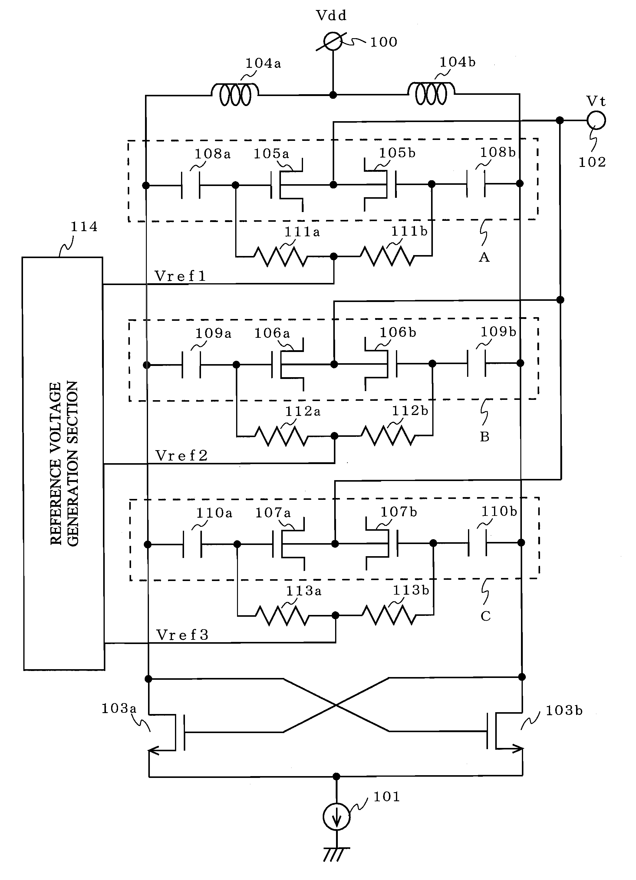
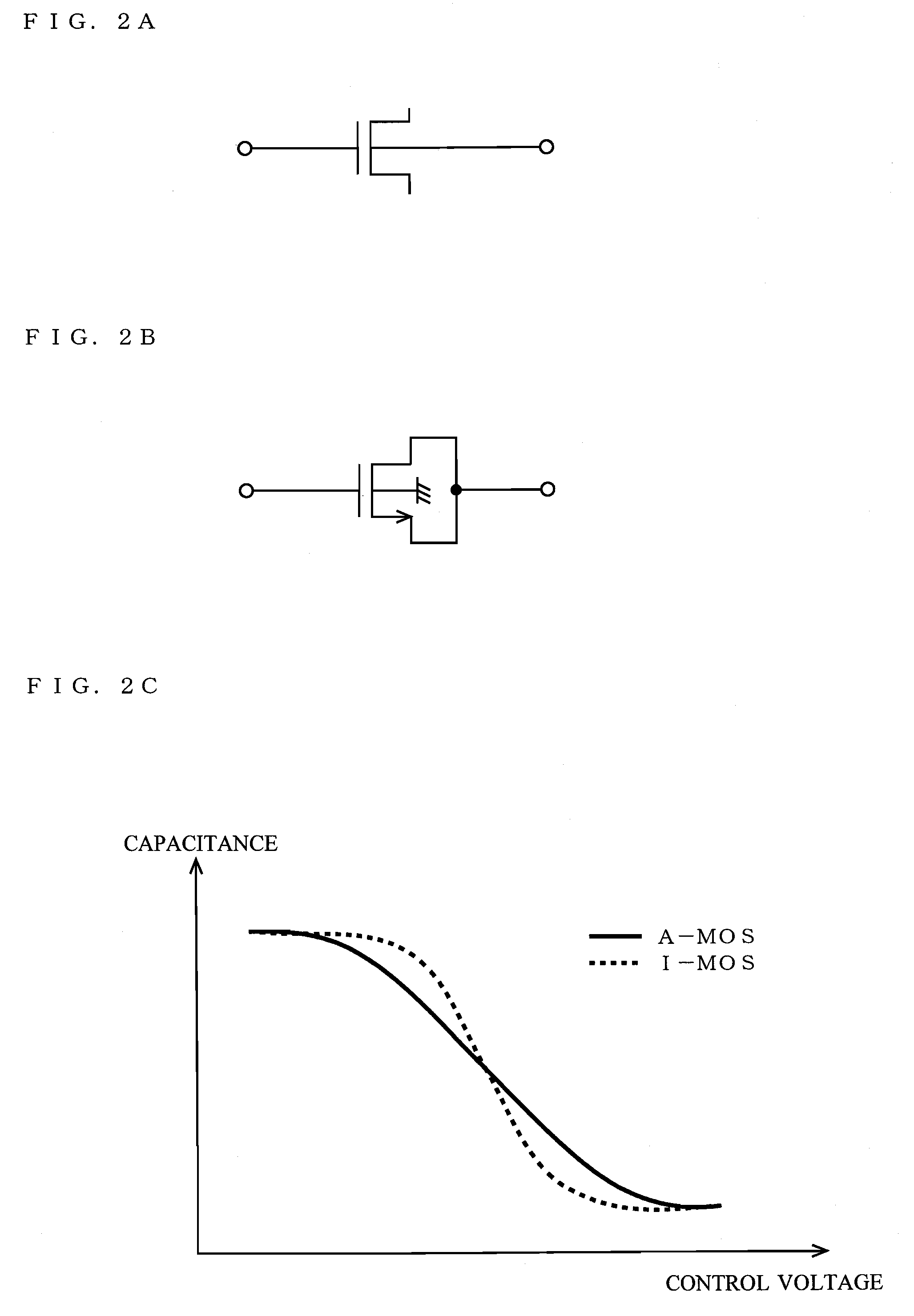
[0066]A voltage difference between the reference voltage Vref1 and the reference voltage Vref2 is represented as V1, and a voltage difference between the reference voltage Vref2 and the reference voltage Vref3 is represented as V2. When V1≠V2, C1a=C2a=C3a, and C1b=C2b=C3b are satisfied, and a capacitance of each of the variable capacitance elements changes in the case of the control voltage Vt being in the neighborhood of Vth, the capacitance value of each of the variable capacitance circuits A, B, and C changes against the control voltage Vt as shown in FIG. 5A. When the voltage difference V1 is set so as to have a value different from the voltage difference V2 as shown in FIG. 5A, a total capacitance of the variable capacitance circuits A, B, and C is able to be proportional to 1 / (fo2) as indicated by the dashed-dotted line in FIG. 5B, thereby improving linear characteristic of a frequency.

[0067]For example, the reference voltages Vref1, Vref2, and Vref3 are s...

example 2

(2) Setting Example 2

[0070]The voltage difference between the reference voltage Vref1 and the reference voltage Vref2 is represented as V1, and the voltage difference between the reference voltage Vref2 and the reference voltage Vref3 is represented as V2. When V1=V2, C2a3a1a, and C2b3b1b are satisfied, and a capacitance of each of the variable capacitance elements changes in the case of the control voltage Vt being in the neighborhood of Vth, a capacitance value of each of the variable capacitance circuits A, B, and C changes against the control voltage Vt as shown in FIG. 9A. When the variable capacitance circuits have capacitance values different from each other, as shown in FIG. 9A, so as to satisfy a value for the variable capacitance circuit A>a value for the variable capacitance circuit C>a value for the variable capacitance circuit B, the total capacitance of the variable capacitance circuits A, B, and C is able to be proportional to 1 / (fo2) as indicated by the dashed-dotted...

example 3

(3) Setting Example 3

[0074]A voltage difference between the reference voltage Vref1 and the reference voltage Vref2 is represented as V1, and a voltage difference between the reference voltage Vref2 and the reference voltage Vref3 is represented as V2. In this case, when V1≠V2, C2a3a1a, and C2b3b1b are satisfied, and a capacitance of each of the variable capacitance elements changes in the case of the control voltage Vt being in the neighborhood of Vth, a capacitance value of each of the variable capacitance circuits A, B, and C changes against the control voltage Vt as shown in FIG. 9A as described for setting example 2. When the voltage difference V1 has a value different from the voltage difference V2, and the variable capacitance circuits have the capacitance values different from each other so as to satisfy a value for the variable capacitance circuit A>a value for the variable capacitance circuit C>a value for the variable capacitance circuit B, the total capacitance of the va...


PUM


Abstract

A voltage controlled oscillator of the present invention comprises a reference voltage generation section 114 for generating a plurality of reference voltage based on a power supply voltage. A first to a third reference voltages Vref1, Vref2, and Vref3 are inputted to a first to a third variable capacitance circuits A, B, and C, respectively, at each one of terminals of each of the first to the third variable capacitance circuits A, B, and C. The first to the third reference voltages Vref1, Vref2, and Vref3 each has a fixed value, and a difference between the first reference voltage Vref1 and the second reference voltage Vref2 and a difference between the second reference voltage Vref2 and the third reference voltage Vref3 represent values different from each other. A control voltage Vt for feedback-controlling an oscillation frequency is inputted to each of the other of the terminals of the variable capacitance element of each of the n variable capacitance circuits such that the control voltage Vt having the same value is inputted to said each of the other of the terminals.

Description

BACKGROUND OF THE INVENTION[0001]1. Field of the Invention[0002]The present invention relates to a voltage controlled oscillator used for generating a local oscillation signal of a radio communication device, and the like, and a PLL circuit and a radio communication apparatus using the same.[0003]2. Description of the Background Art[0004]A voltage controlled oscillator (VCO) is widespread as a device for generating a local oscillation signal of a radio communication device. FIG. 14 is a diagram illustrating an exemplary configuration of a conventional voltage controlled oscillator. The conventional voltage controlled oscillator includes: an inductor 604a and an inductor 604b; a variable capacitance element 605a and a variable capacitance element 605b; an oscillation transistor 603a and an oscillation transistor 603b; and a current source 601. In FIG. 14, a bias circuit and the like are not shown.[0005]The inductor 604a and the inductor 604b, and the variable capacitance element 605a...

Claims


Application Information

Patent Timeline
Patent Type & Authority Applications(United States)
IPC IPC(8): H03B7/06
CPCH03B2201/025H03J2200/10H03B5/1228H03B5/1293H03B5/1243H03B5/1265H03B5/1215
Inventor TSUKIZAWA, TAKAYUKITAKINAMI, KOJI
Owner PANASONIC CORP
Why Eureka
Try Eureka