Semiconductor circuit

a technology of semiconductors and circuits, applied in the direction of pulse techniques, instruments, process and machine control, etc., can solve the problems of power loss, affecting the operation of the whole system, and destroying the power switching elements and sometimes the whole system, so as to prevent an erroneous operation, reduce power loss, and reduce the effect of loss

Inactive Publication Date: 2008-08-28
HITACHI LTD
View PDF5 Cites 24 Cited by
  • Summary
  • Abstract
  • Description
  • Claims
  • Application Information

AI Technical Summary

Benefits of technology

[0010]Also, in a semiconductor circuit according to this invention, two power switching elements are used as an upper arm power switching element and a lower arm power switching element provided between a high voltage terminal and a reference voltage terminal; a load is connected with the terminal between the upper arm power switching element and the lower arm power switching element; and a dead time is provided between the second control signal for the upper arm power switching element and the second control signal for the lower arm power switching element, so as to prevent the upper arm power switching element and the lower arm power switching element from being turned on simultaneously in the normal drive mode.
[0015]In a semiconductor circuit according to this invention, the dead time can be shortened to its minimal limit while preventing an erroneous operation that may be caused as a result of the synchronous rectifying drive. Accordingly, the resulted bridge circuit can be applied to high frequency, low loss operations.
[0016]In a semiconductor circuit according to this invention, since free wheel diodes can be dispensed with, the reduction of size and cost will also be possible.

Problems solved by technology

Accordingly, there arises a possibility that large current flows from the high voltage source terminal to the ground to destroy the power switching elements and sometimes the whole system.
However, if the dead time is too long, it causes an increase in power loss so that high frequency application is hardly possible.
This is a drawback with this system.

Method used


Image

  • Semiconductor circuit
  • Semiconductor circuit
  • Semiconductor circuit

Examples


embodiment 1

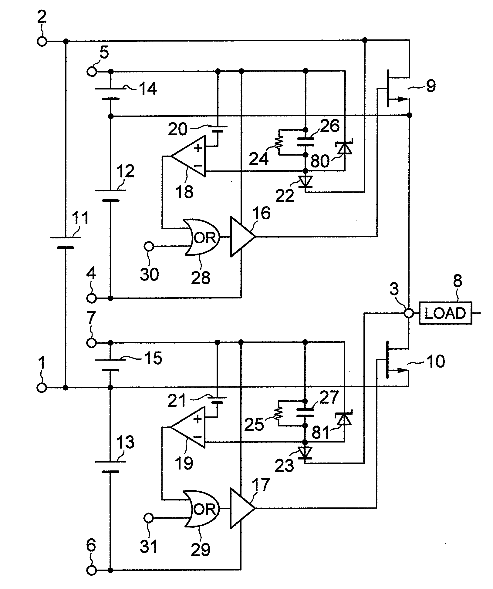
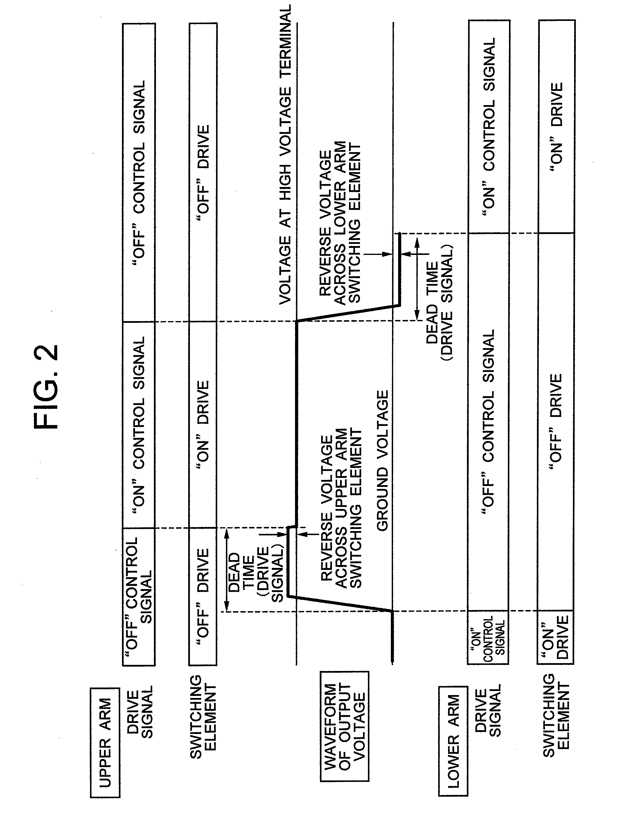
[0040]FIG. 1 shows a semiconductor circuit as a first embodiment of this invention, FIG. 2 shows a diagram for illustrating how an example of the conventional drive system operates, and FIG. 3 shows a diagram for illustrating how the semiconductor circuit shown in FIG. 1 operates. This embodiment is described below on the assumption that the drive period is long, the inductive energy stored in the load while the “on” pulse is being applied is released, and no backflow current exists at the end of the “on” pulse. It is also assumed in the following description that the power switching element 9 of the upper arm and the power switching element 10 of the lower arm are n-channel JFETs (junction type field effect transistors) in most cases. However, this assumption does not mean the exclusion of the use of other power switching elements such as power MOSFETs or bipolar transistors in place of the JFETs.

[0041]The semiconductor circuit shown in FIG. 1 has a ground terminal 1, the high volt...

embodiment 2

[0053]FIGS. 4 and 5 show diagrams for illustrating how a semiconductor circuit as the second embodiment of this invention operates when the output voltage rises and falls, respectively. The semiconductor circuit as this second embodiment is the same as the semiconductor circuit shown as the first embodiment in FIG. 1, but characterized in that the synchronous rectifying drive is initiated before the end of the switching period. It is therefore possible to eliminate the period during which the voltage at the output terminal 3 rises far above the voltage of the high voltage source and falls far below the ground voltage, after the end of switching. This way of driving can be effected by suitably choosing the values of the reference voltages 20, 21 applied to the positive terminals of the comparators 18, 19. Alternatively, the same way of driving can be realized, as described above in the first embodiment, by determining the condition for the synchronous rectifying drive due to the firs...

embodiment 3

[0055]FIG. 6 shows a semiconductor circuit as a third embodiment of this invention. In this embodiment, state holding circuits are provided after the output terminals of the comparator 18, 19 to fulfill the intended purpose. Namely, diodes 100, 101, resistors 96, 97, and capacitors 98, 99 constitute the state holding circuits. The state holding circuits provided before the negative terminals of the comparator circuits 18, 19 as shown in the first embodiment in FIG. 1 are also employed in this embodiment so as to enhance the precision in the operation of the state holding circuits. However, one of the state holding circuits provided before and after each comparator circuit may be dispensed with.

[0056]This embodiment can enjoy the same advantage as the first embodiment can.


PUM


Abstract

A synchronous rectifying drive type semiconductor circuit wherein voltages between drains and sources of power switching elements are detected, temporarily held and compared with a reference voltage. First control signals are generated for turning on the power switching elements depending on comparison result and dead times for the power switching elements are minimized by ORing first control signals and second control signals inputted at input terminals. The first control signals cause the power switching elements to be in “on” state for a constant time until the second control signals as “on” control signals arrive at the input terminals, and then the first control signals as “on” control signals are terminated before the second control signals as “off” signals arrive at the input terminals, thereby swiftly turning off the power switching elements by the second control signals arriving at the input terminals.

Description

BACKGROUND OF THE INVENTION[0001]This invention relates to a synchronous rectifying drive system wherein current flows through the power switching elements in the reverse direction as well as in the forward direction, and more particularly to a semiconductor circuit capable of performing switching control with low power loss.[0002]In the case of driving an inductive load, there are two modes: the recirculation mode wherein electric energy stored in the inductive load causes electric currents to flow through the power switching elements in the reverse direction and the normal mode wherein electric currents flow through the power switching elements in the forward direction. In the synchronous rectifying drive system, the power switching elements are reversely operated, i.e. turned on in the recirculation mode wherein the reverse voltages are applied to the power switching elements, so that voltage drops across the power switching elements are suppressed as much as possible. However, i...

Claims


Application Information

Patent Timeline
Patent Type & Authority Applications(United States)
IPC IPC(8): H02M7/06
CPCH02M3/07H02M3/1588H02M2003/1555H03K17/165Y02B70/1466H03K17/691H03K17/785H03K2017/6875H03K2217/0036H03K17/6871Y02B70/10H02M3/1555
Inventor SAKAMOTO, KOZO
Owner HITACHI LTD
Why Eureka
Try Eureka