Relief printing plate, and method for manufacturing electronic circuit pattern, organic electroluminescence device and organic electronic device by using the same

a technology of electronic circuit pattern and printing plate, which is applied in the direction of photomechanical equipment, instruments, photosensitive materials, etc., can solve the problems of increasing the size of the substrate, reducing the patterning accuracy, and not being practicable for organic el devices

Inactive Publication Date: 2008-08-28
TOPPAN PRINTING CO LTD
View PDF6 Cites 15 Cited by
  • Summary
  • Abstract
  • Description
  • Claims
  • Application Information

AI Technical Summary

Problems solved by technology

Since there was a problem in a light emitting efficiency, the organic EL device was not in practical use.
However, this method has a problem that patterning accuracy is reduced with an increase in size of a substrate.
However, in view of accuracy of a mask, if a substrate to be evaporated is large, it is difficult to form a pattern.
In other case, since accuracy in dropping of an ink droplet is bad, there is a problem in than a linear pattern can not obtained.
However, when the repelled ink goes back inside a pixel, an ink is built up, thereby there is a remained problem in that a fluctuation of film thickness of an organic light emitting layer inside a pixel occurs.
However, the wet coating methods have difficulty in realizing the high definition patterning and color coding with R, G, and B, and it is considered that the thin film is most effectively formed by a printing process that is capable of achieving excellent color coding and patterning.
Thus, a method to use metal hard printing plate such as a gravure printing method is unsuitable.
In this case, if a relief printing plate has a defect, a pattern printed on a substrate by using this relief printing plate also has a defect.
This causes a defective device.
If shapes of the patterns are different, it is thought that a defect such as an included undesirable material or a void in a pixel occurs.
The characteristics of the organic electroluminescence device may become bad by irradiation light at the time of the checking.
In addition, if the characteristics do not become bad, it is difficult to check the device because it is difficult to obtain sufficient contrast at the time of optical checking.
However, in the case where the defect check is performed for a fine pattern on a metal substrate by a comparison checking, it is difficult to recognize a defect.

Method used


Image

  • Relief printing plate, and method for manufacturing electronic circuit pattern, organic electroluminescence device and organic electronic device by using the same
  • Relief printing plate, and method for manufacturing electronic circuit pattern, organic electroluminescence device and organic electronic device by using the same
  • Relief printing plate, and method for manufacturing electronic circuit pattern, organic electroluminescence device and organic electronic device by using the same

Examples


example

[0233]Hereinafter, an example is described.

(Manufacturing a Substrate to be Printed)

[0234]An active matrix substrate having a thin film transistor provided on a supporting body, the transistor functioning as a switching device, a planarizing layer formed over the transistor and a pixel electrode on the planarizing layer, the electrode being electrically connected with the thin film transistor through a contact hole was used for a substrate to be printed. As for the size of the substrate, the diagonal size was 1.8 inch. The number of pixels was 64×64.

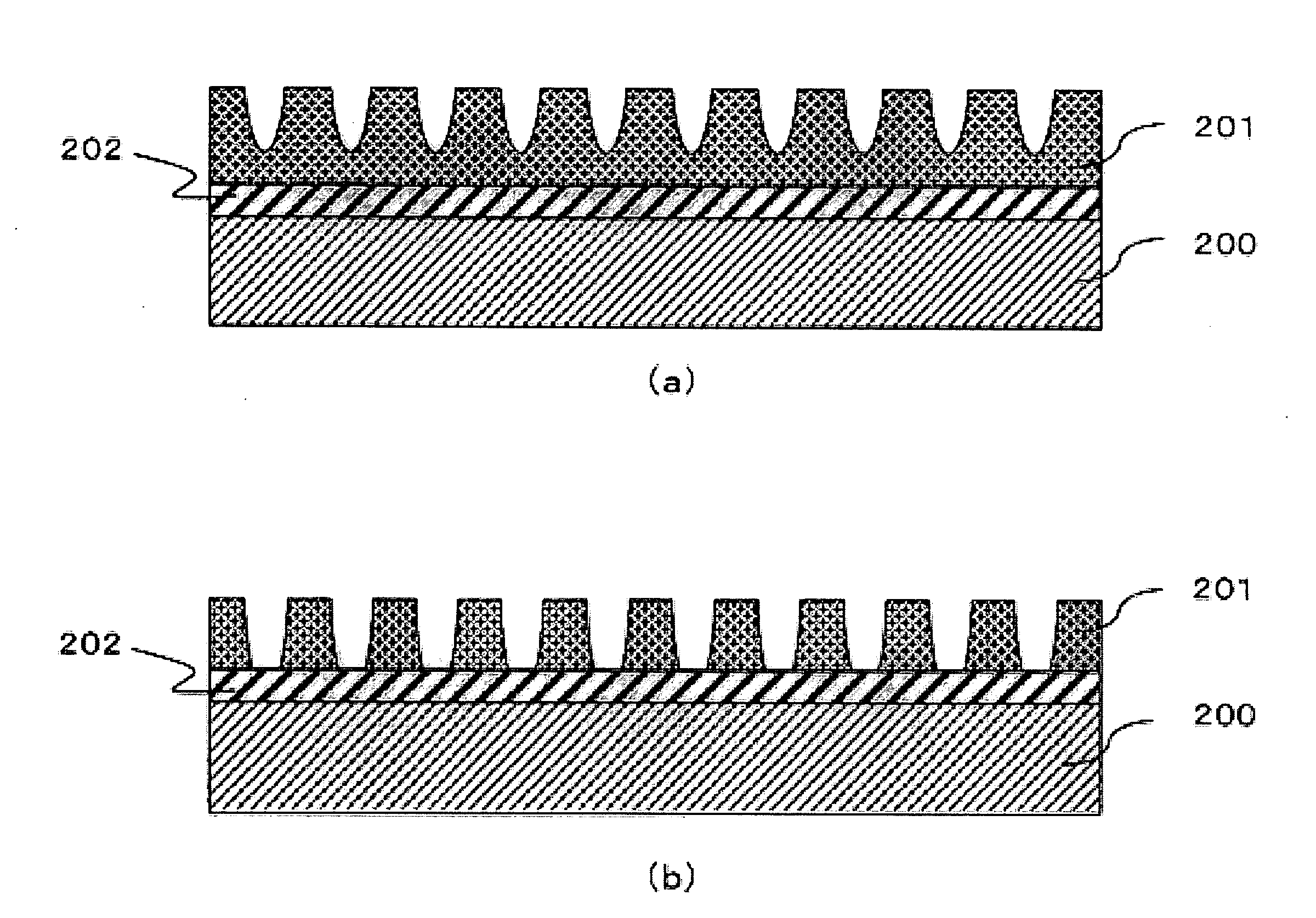
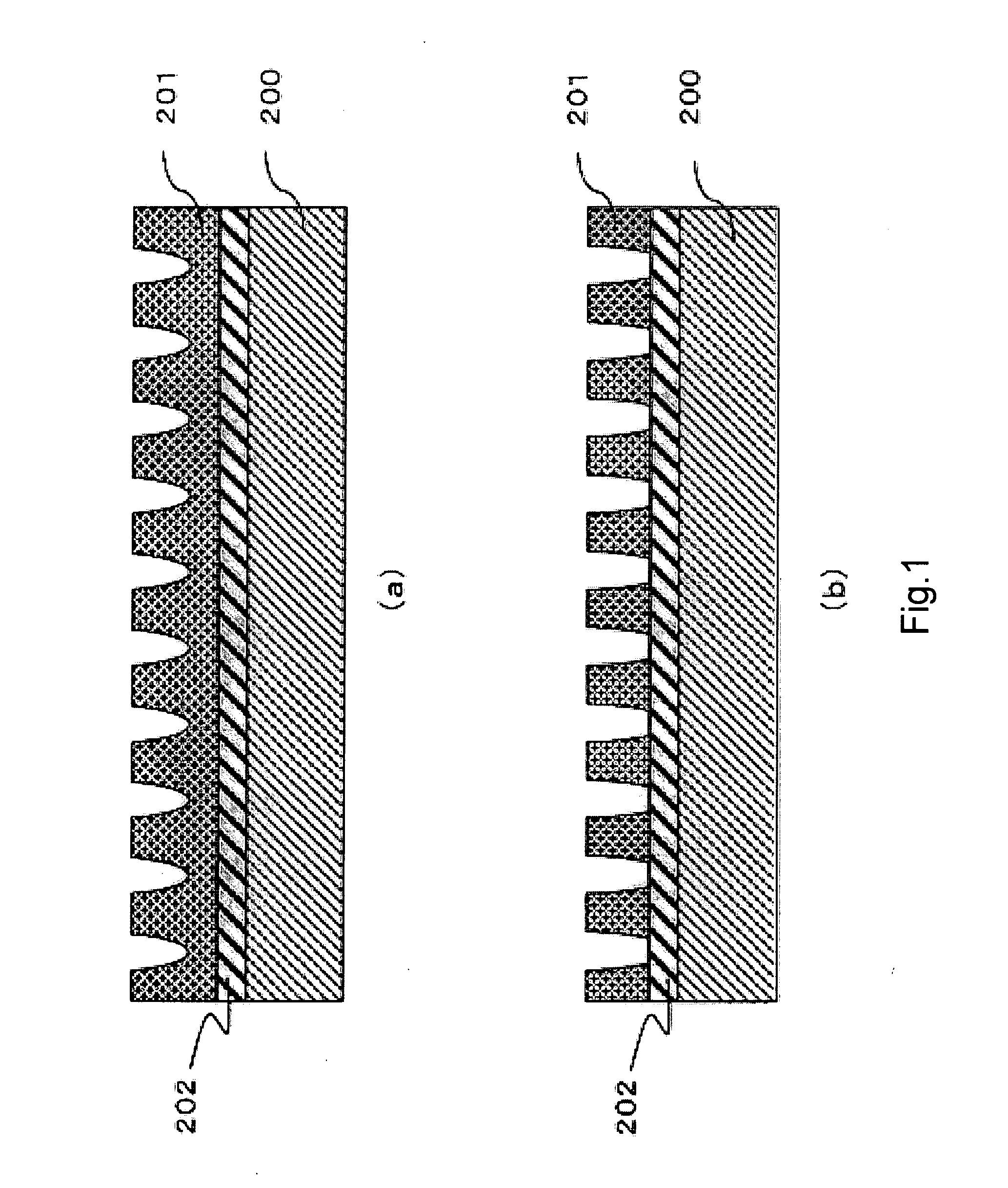
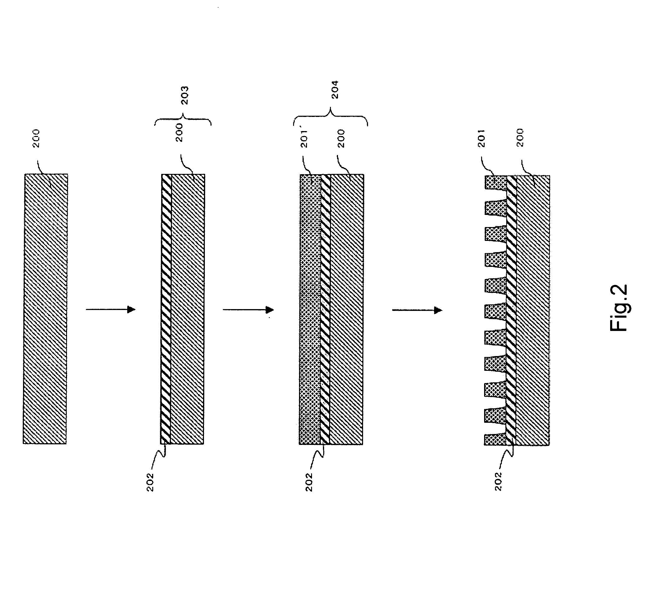
[0235]A partition wall was formed so that the shape of the partition wall makes it possible to cover an end of the pixel electrode provided on this substrate and to section pixels. The partition wall was formed by the following processes: a positive resist (ZWD6216-6: a product of ZEON CORPORATION) was formed on the entire surface of the substrate by a spin coater so that thickness of the resist was 2 μm; and the partition wall having wi...


PUM

PropertyMeasurementUnit
transmittanceaaaaaaaaaa
thicknessaaaaaaaaaa
sizeaaaaaaaaaa

Abstract

An embodiment of the present invention is a relief printing plate for forming a high-definition pattern by a printing method, having a convex part comprising a resin layer, a base material supporting the convex part and a light reflection controlling layer, the light wave length being in range of 400 nm-800 nm, and the layer being between the convex part and the base material.

Description

CROSS REFERENCE[0001]This application claims priority to Japanese application number 2007-033337, filed on Feb. 14, 2007, and priority to Japanese application number 2007-070261, filed on Mar. 19, 2007, which are incorporated by references.BACKGROUND OF THE INVENTION[0002]1. Field of the Invention[0003]The present invention is related to the following products or methods:[0004](A) a relief printing plate for forming a high definition pattern by a printing method;[0005](B) a plate type photosensitive resin for manufacture the relief printing plate;[0006](C) a method for manufacturing an electric circuit pattern formed using the relief printing plate;[0007](D) a method for manufacturing an organic electroluminescence (EL) device;[0008](E) an organic EL device; and[0009](F) an organic EL display.[0010]In addition, the present invention is related to the following products or methods:[0011](G) a relief printing plate used for manufacturing an organic electronic device;[0012](H) an inspe...

Claims


Application Information

Patent Timeline
Patent Type & Authority Applications(United States)
IPC IPC(8): G03F7/20G03F7/004
CPCH01L47/00H01L51/0004H05K2203/0108H05K3/1275H01L51/0022H10N80/00H10K71/13H10K71/611
Inventor KAWAKAMI, HIRONORITAKESHITA, KOJISHIMIZU, TAKAHISAINOKUCHI, NAHOKOIRIE, KAZUNOBU
Owner TOPPAN PRINTING CO LTD
Why Eureka
Try Eureka