Exposure method, method for manufacturing flat panel display substrate, and exposure apparatus

Inactive Publication Date: 2008-08-28
NIKON CORP
View PDF22 Cites 9 Cited by
  • Summary
  • Abstract
  • Description
  • Claims
  • Application Information

AI Technical Summary

Benefits of technology

[0007]However, the enlargement of masks results in an increase in the size and cost of the masks. Further, the size and cost of transportation, storage, and washing apparatuses for the mask, and the like are increased. This increases the manufacturing cost of the flat panel displays.
[0008]Accordingly, it is a first object of the present invention to provide an exposure method for forming

Problems solved by technology

However, the enlargement of masks results in an increase in the size and cost of the masks.
Further, the size and cost of transportation, s

Method used


Image

  • Exposure method, method for manufacturing flat panel display substrate, and exposure apparatus
  • Exposure method, method for manufacturing flat panel display substrate, and exposure apparatus
  • Exposure method, method for manufacturing flat panel display substrate, and exposure apparatus

Examples


Embodiment Construction

[0025]One embodiment of the present invention will now be discussed.

[0026]Hereinafter, a pattern represents the shape of a bright-dark distribution formed by exposure light.

[0027]Further, a mask pattern represents the distribution shape of one or both of a light transmission portion and light shielding portion formed on a mask.

[0028]An exposure pattern represents the exposure distribution shape exposed onto a photosensitive material, such as photoresist, that is formed on a substrate.

[0029]A substrate pattern represents at least part of a conductive member, an insulative member, or a semiconductor member formed on a substrate.

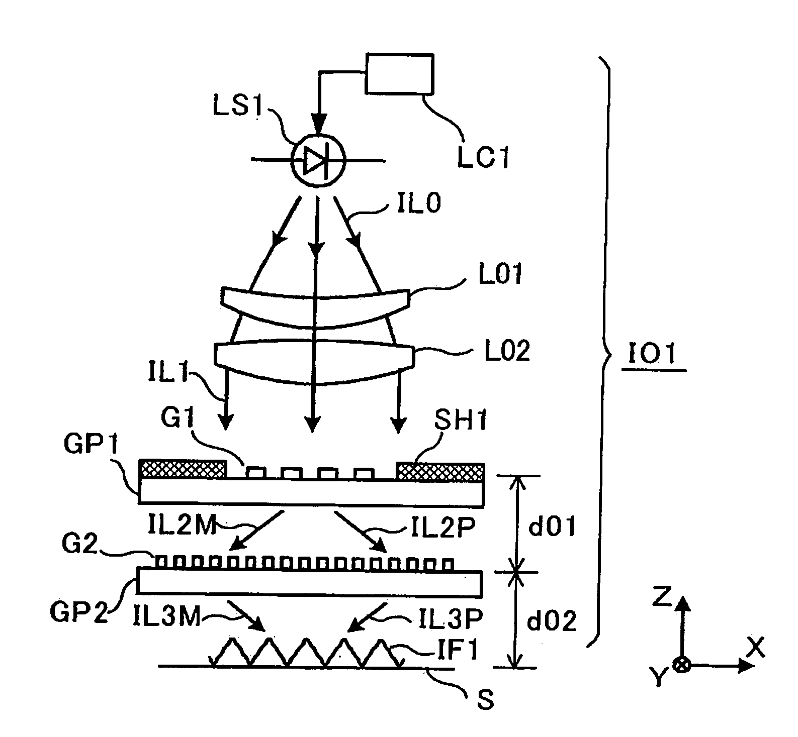
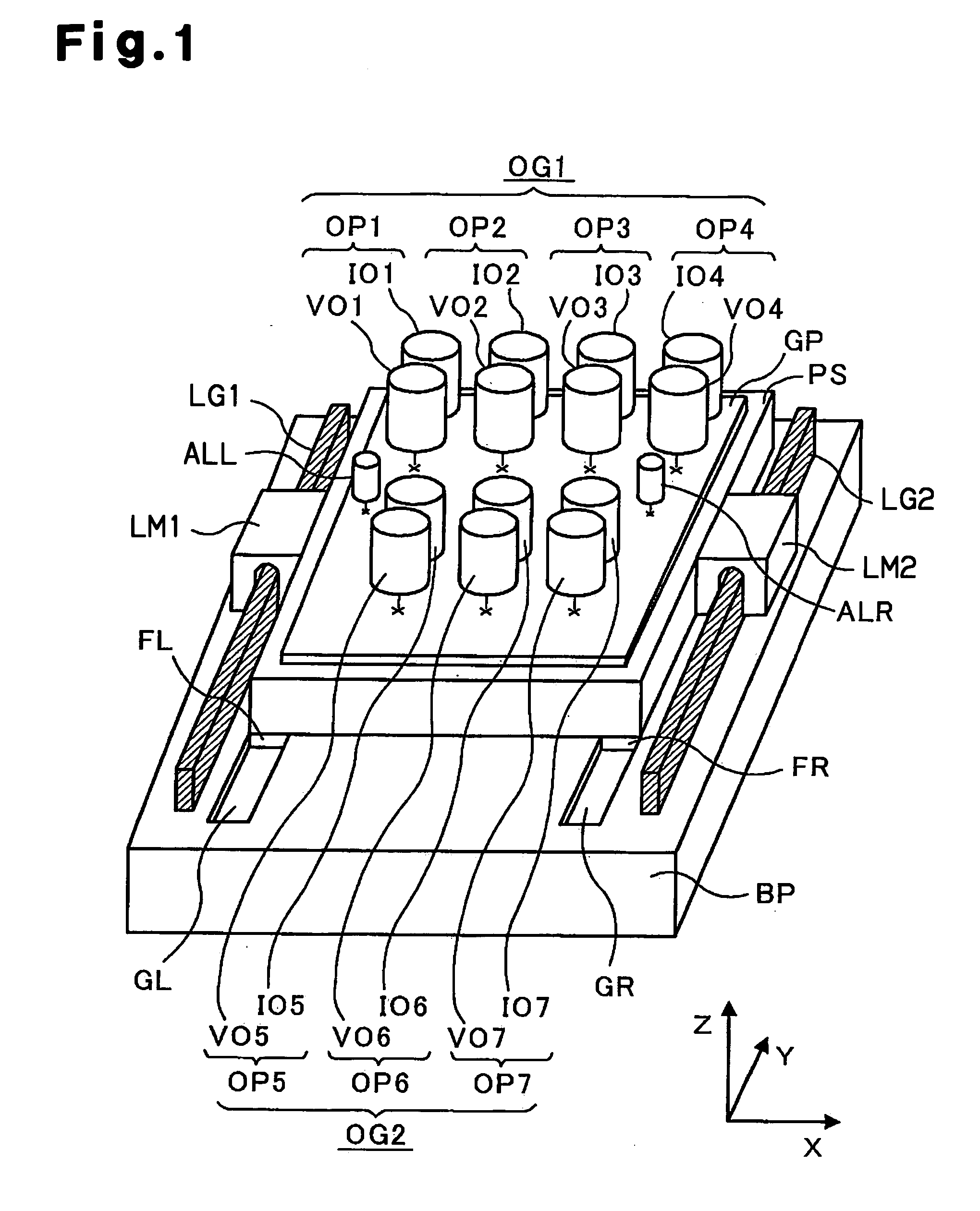
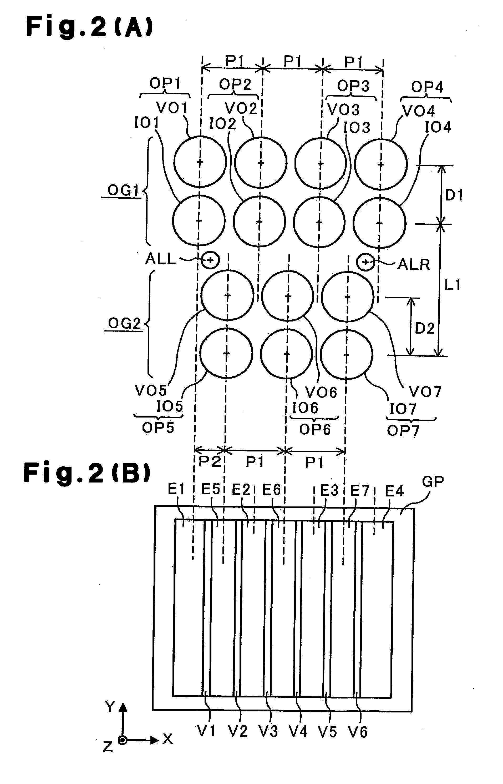
[0030]FIG. 1 is a diagram showing a first example of an exposure apparatus according to the present invention.

[0031]A substrate stage PS holds a substrate GP, such as a glass substrate that forms a picture display portion of a flat panel display.

[0032]Above the substrate stage PS (+Z direction as viewed in the drawing), a first exposure optical group OG1 and a ...


PUM


Abstract

An exposure method and exposure apparatus optimal for the formation of a fine pattern of an electronic device, such as a flat panel display. The exposure method and apparatus provides a high resolution and is inexpensive. The exposure method exposes a pattern onto a substrate with the use of an optical system that performs interference exposure for exposing a pattern parallel to a predetermined scanning direction with an interference optical system and variable shaping exposure with a variable shaping optical system while performing relative scanning in the scanning direction.

Description

BACKGROUND OF THE INVENTION[0001]The present invention relates to an exposure method used during a fine pattern formation step in a manufacturing process of a substrate that forms a picture display unit of a flat panel display. The present invention further relates to an optical exposure method and exposure apparatus that uses the manufacturing method.[0002]During a process for manufacturing a substrate used as a flat panel display, such as a liquid crystal display or a plasma display, when forming a fine pattern on the substrate, photolithography is normally implemented. Photolithography forms a preferable pattern shape on the substrate by forming a photosensitive film (photoresist) on the surface of the substrate and performing an exposure step for exposing the substrate with exposure light having a light distribution that is in accordance with the shape of a pattern that is to be formed. Then, a development step, an etching step, and the like are performed.[0003]In the prior art,...

Claims


Application Information

Patent Timeline
IPC IPC(8): G03B27/42G03F7/20B05D5/12
CPCG03F7/70391G03F7/70466G03F7/7045G03F7/70408G03F7/7055
Inventor SHIRAISHI, NAOMASA
Owner NIKON CORP
Why Eureka
Try Eureka