Methods of reducing impurity concentration in isolating films in semiconductor devices

a technology of isolating film and semiconductor device, which is applied in the direction of air heater, heating type, lighting and heating apparatus, etc., can solve the problems of reducing device characteristics, relatively high impurity density, and/or relatively high etching rate, and achieve the effect of reducing the impurity concentration of the film

Active Publication Date: 2008-08-28
SAMSUNG ELECTRONICS CO LTD
View PDF30 Cites 33 Cited by
  • Summary
  • Abstract
  • Description
  • Claims
  • Application Information

AI Technical Summary

Benefits of technology

[0005]According to some embodiments of the present invention, a method of fabricating a semiconductor device includes forming a first device on a first semiconductor substrate. An interlayer insulating film is formed on the first device, and a second semiconductor substrate is formed on the interlayer insulating film such that the interlayer insulating film is between the first and second semiconductor substrates. Trenches are formed within the second semiconductor substrate, and a device isolating film is formed within the trenches. The device isolating film is irradiated with ultraviolet light having a wavelength configured to break chemical bonds of impurities in the device isolating film to reduce an impurity concentration thereof.

Problems solved by technology

However, such a film may have a relatively high impurity density and / or a relatively high etching rate as-deposited.
Thus, device characteristics may be degraded during such a furnace annealing process.

Method used


Image

  • Methods of reducing impurity concentration in isolating films in semiconductor devices
  • Methods of reducing impurity concentration in isolating films in semiconductor devices
  • Methods of reducing impurity concentration in isolating films in semiconductor devices

Examples


Embodiment Construction

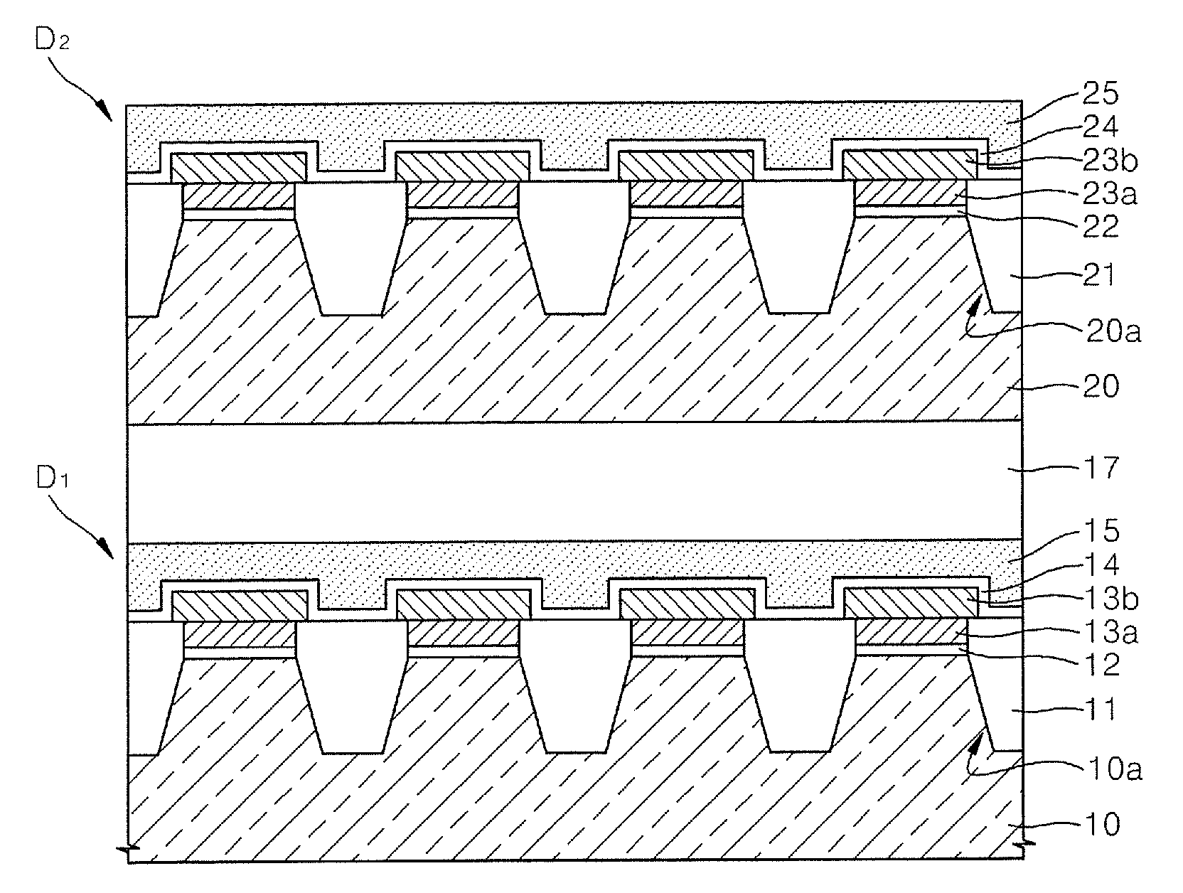
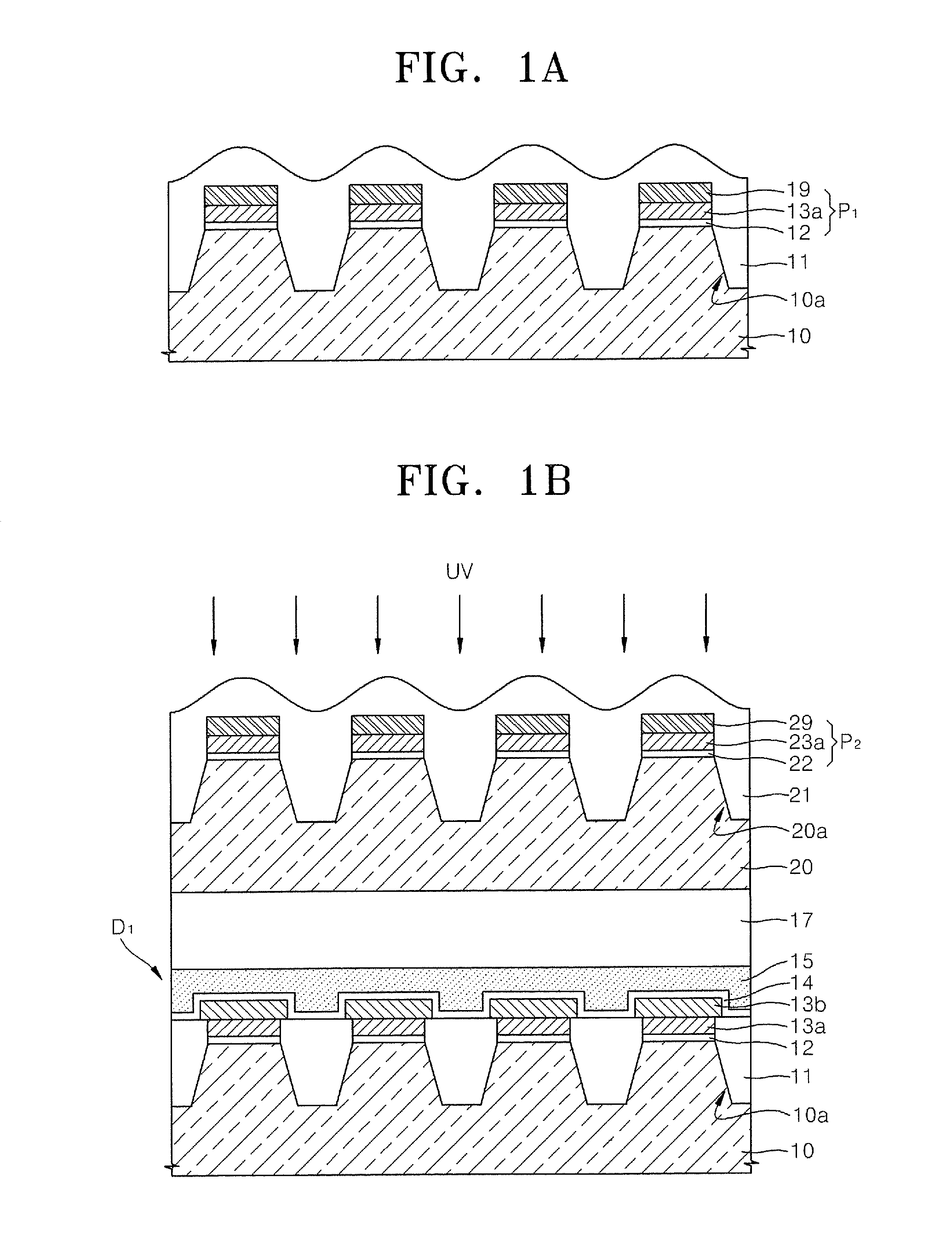
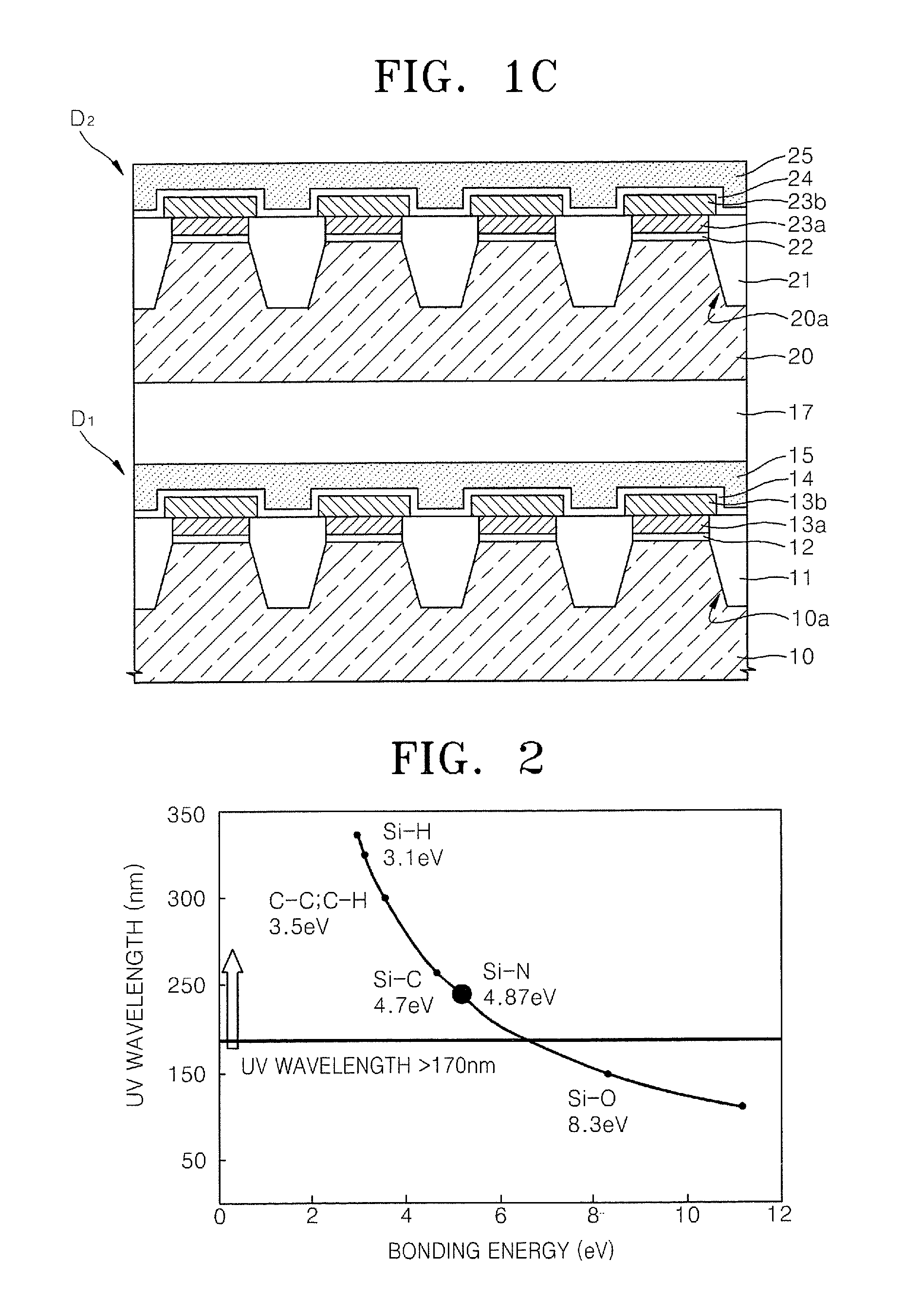
[0021]The present invention will now be described more fully hereinafter with reference to the accompanying drawings, in which embodiments of the invention are shown. This invention, however, may be embodied in many different forms and should not be construed as limited to the embodiments set forth herein. Rather, these embodiments are provided so that this disclosure will be thorough and complete, and will fully convey the scope of the invention to those skilled in the art. In the drawings, the thicknesses of layers and regions are exaggerated for clarity. Like numbers refer to like elements throughout.

[0022]It will be understood that when an element or layer is referred to as being “on”“connected to” or “coupled to” another element or layer, it can be directly on, connected or coupled to the other element, or layer or intervening elements or layers may be present. In contrast, when an element is referred to as being “directly on,”“directly connected to” or “directly coupled to” an...


PUM


Abstract

A method of fabricating a semiconductor device includes forming a lower device on a lower semiconductor substrate, and forming an interlayer insulating film on the lower device. An upper semiconductor substrate is formed on the interlayer insulating film such that the interlayer insulating film is between the lower and upper semiconductor substrates. Upper trenches are formed within the upper semiconductor substrate. An upper device isolating film is formed within the upper trenches. The upper device isolating film is irradiated with ultraviolet light having a wavelength configured to break chemical bonds of impurities in the upper device isolating film to reduce an impurity concentration thereof.

Description

CROSS-REFERENCE TO RELATED PATENT APPLICATIONS[0001]This application claims priority from Korean Patent Application No. 10-2007-0019879, filed on Feb. 27, 2007, in the Korean Intellectual Property Office, the disclosure of which is incorporated by reference herein in its entirety.FIELD OF THE INVENTION[0002]The present invention relates to a method of fabricating semiconductor devices, and more particularly to methods of fabricating insulating films in semiconductor devices.BACKGROUND OF THE INVENTION[0003]Semiconductor devices typically include a plurality of elements, such as transistors, formed on a semiconductor substrate. In order to electrically isolate these elements, a film such as a spin on glass (SOG) film having relatively good gap-filling characteristics may be used. However, such a film may have a relatively high impurity density and / or a relatively high etching rate as-deposited. Therefore, a furnace annealing process performed at a relatively high temperature may be u...

Claims


Application Information

Patent Timeline
Patent Type & Authority Applications(United States)
IPC IPC(8): H01L21/762
CPCH01L21/823481H01L21/76224A01G9/24F24D5/08F24H3/08F24H9/0068
Inventor CHOI, JONG-WANBAEK, EUN-KYUNGAHN, SANG-HOONKIM, HONG-GUNSUH, DONG-CHULCHOI, YONG-SOON
Owner SAMSUNG ELECTRONICS CO LTD
Why Eureka
Try Eureka