Organic Electroluminescence Device Having Input Function and Electronic Apparatus

a technology of electroluminescence device and electronic apparatus, which is applied in the direction of static indicating device, discharge tube luminescnet screen, instruments, etc., can solve the problems of reducing conceivable problem of contact position detection error, and image quality degradation, so as to prevent the accuracy of contact position detection from being lowered, the effect of increasing reliability and enhancing performan

Active Publication Date: 2008-09-04
ELEMENT CAPITAL COMMERCIAL CO PTE LTD
View PDF14 Cites 53 Cited by
  • Summary
  • Abstract
  • Description
  • Claims
  • Application Information

AI Technical Summary

Benefits of technology

[0008]An advantage of some aspects of the invention is to provide an organic EL device that is capable of preventing the precision in contact position detection from being lowered because of an electric field noise that is generated when organic EL elements are driven for light emission. In addition, the invention further provides, advantageously, an electronic apparatus that is provided with such a high-performance organic EL device to offer reliable contact position detection with enhanced detection accuracy.
[0010]In the configuration of the organic electroluminescence device having an input function according to the first aspect of the invention described above, the shield conductor is formed on the element-substrate side of the sealing substrate. In addition, there is a gap between one negative electrode and another (i.e., adjacent one) negative electrode, where the negative electrode is formed on an individual basis so as to correspond to the display color of each of the sub pixel regions. With such a configuration, the shield conductor shuts off an electric field that was generated at the time of emission of light from the light-emitting layer and then propagates to leak through a gap between two adjacent ones of the negative electrodes toward the touch panel section. Therefore, it is possible to reduce the adverse effects of an electric field noise exerted onto the functioning of the touch panel section, where the electric field is generated by a driving signal supplied for the emission of light, thereby making it further possible to improve the accuracy in the contact detection of a touch panel user input made at the touch panel section. Thus, the invention makes it possible to provide an organic EL device that is capable of preventing the precision in contact position detection from being lowered because of an electric field noise that is generated when organic EL elements are driven for light emission.
[0011]In the configuration of the organic electroluminescence device having an input function according to the first aspect of the invention described above, it is preferable that the shield conductor should constitute a light-shielding film. If so configured, the shield conductor also functions as the light-shielding film. Therefore, it is possible to reduce the number of parts and components that make up the sealing substrate, thereby making it possible to reduce the thickness of the sealing substrate. In addition to the above, since the shield conductor is provided only at regions where the light-shielding film is formed, optical output efficiency is not sacrificed.
[0013]With such a configuration, it is possible to form the shield conductor in a planar pattern on the condition that the shield conductor is made of an electro-conductive material having optical transparency. Thus, it is possible to effectively and reliably block the adverse effects of a noise at the time of light emission.
[0014]In the configuration of the organic electroluminescence device having an input function according to the first aspect of the invention described above, it is preferable that the shield conductor should have a light-transmissive portion that is formed in a planar pattern on the image display area of the sealing substrate and a light-shielding portion that functions as a light-shielding film. In order to heighten the light transmission factor of the light-transmissive portion, it is necessary to make the film thickness of the light-transmissive portion smaller. If done so, however, the resistance value of shield conductor increases, which is undesirable. Nevertheless, it is possible to adjust the resistance value of the shield conductor as a whole by adjusting the film thickness of the light-shielding portion because the light-shielding portion does not have to have optical transparency. That is, in the preferred configuration of the organic EL device having an input function according to the first aspect of the invention described above, it is possible to counterbalance an increase in the resistance value due to the reduced film thickness of the light-transmissive portion with a decrease in the resistance value obtained by adjusting the film thickness of the light-shielding portion. By this means, it is possible to maintain the resistance value of the shield conductor as a whole at a predetermined value. In addition, since the light-shielding portion is formed in a planar pattern to demarcate the image display area, it is possible to effectively and reliably block the adverse effects of a noise. Moreover, since the light-shielding portion is configured to have a small film thickness, it is possible to output light that is emitted from the light-emitting layer to the outside with high optical efficiency. Moreover, in the preferred configuration of the organic EL device having an input function according to the first aspect of the invention described above, the light-shielding portion makes it possible to avoid the occurrence of optical leakage through a gap between each two adjacent ones of the plurality of sub pixel regions.
[0016]Since the electronic apparatus according to the second aspect of the invention is provided with, for example as its display unit, the organic electroluminescence device having an input function that is capable of preventing the precision in contact position detection from being lowered because of an electric field noise that is generated when organic EL elements are driven for light emission, the electronic apparatus features greater performance in the detection of a touch panel user input with an increased reliability.

Problems solved by technology

Since an organic EL element is a device (i.e., element) that is driven by an electric current, any variation or fluctuation in a driving electric current supplied thereto leads directly to the degradation of image quality.
However, in the configuration of such a touch-sensitive organic EL device that combines a touch panel configuration conforming to the capacitive sensing scheme with an individual R, G, and B negative electrode configuration described above, there is a conceivable problem of a contact position detection error due to an electric field noise.
That is, since an electric field, which is generated by a driving signal that is supplied between a pair of electrodes for driving an organic EL element for light emission, undesirably reaches a detection electrode through a gap region between each two adjacent ones of the individual R, G, and B negative electrodes, the accuracy in the detection of a contact position decreases because of the electric field component that disturbs the functioning of the detection electrode as a noise.
If done so, however, the resistance value of shield conductor increases, which is undesirable.

Method used


Image

  • Organic Electroluminescence Device Having Input Function and Electronic Apparatus
  • Organic Electroluminescence Device Having Input Function and Electronic Apparatus
  • Organic Electroluminescence Device Having Input Function and Electronic Apparatus

Examples


first embodiment

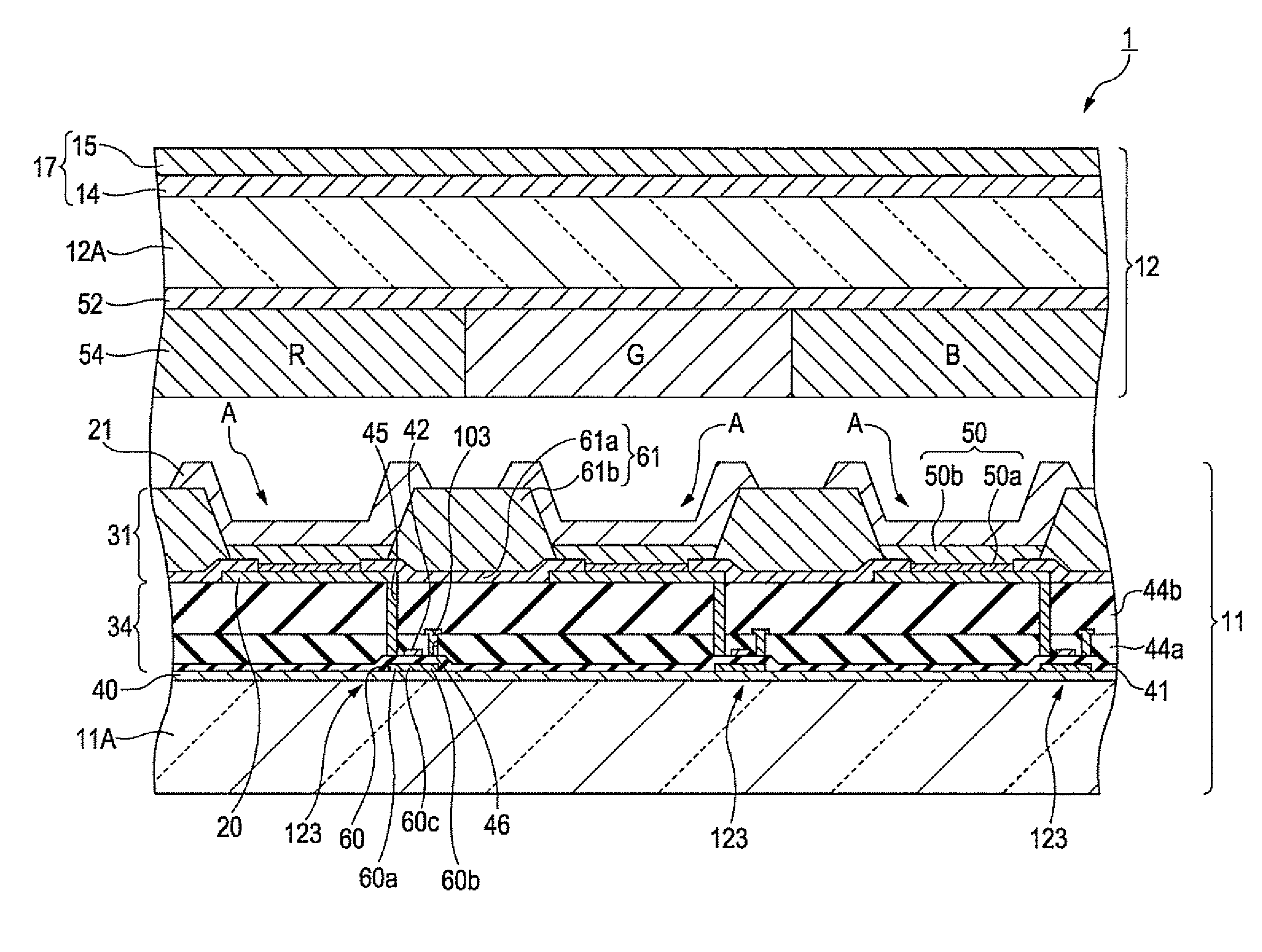
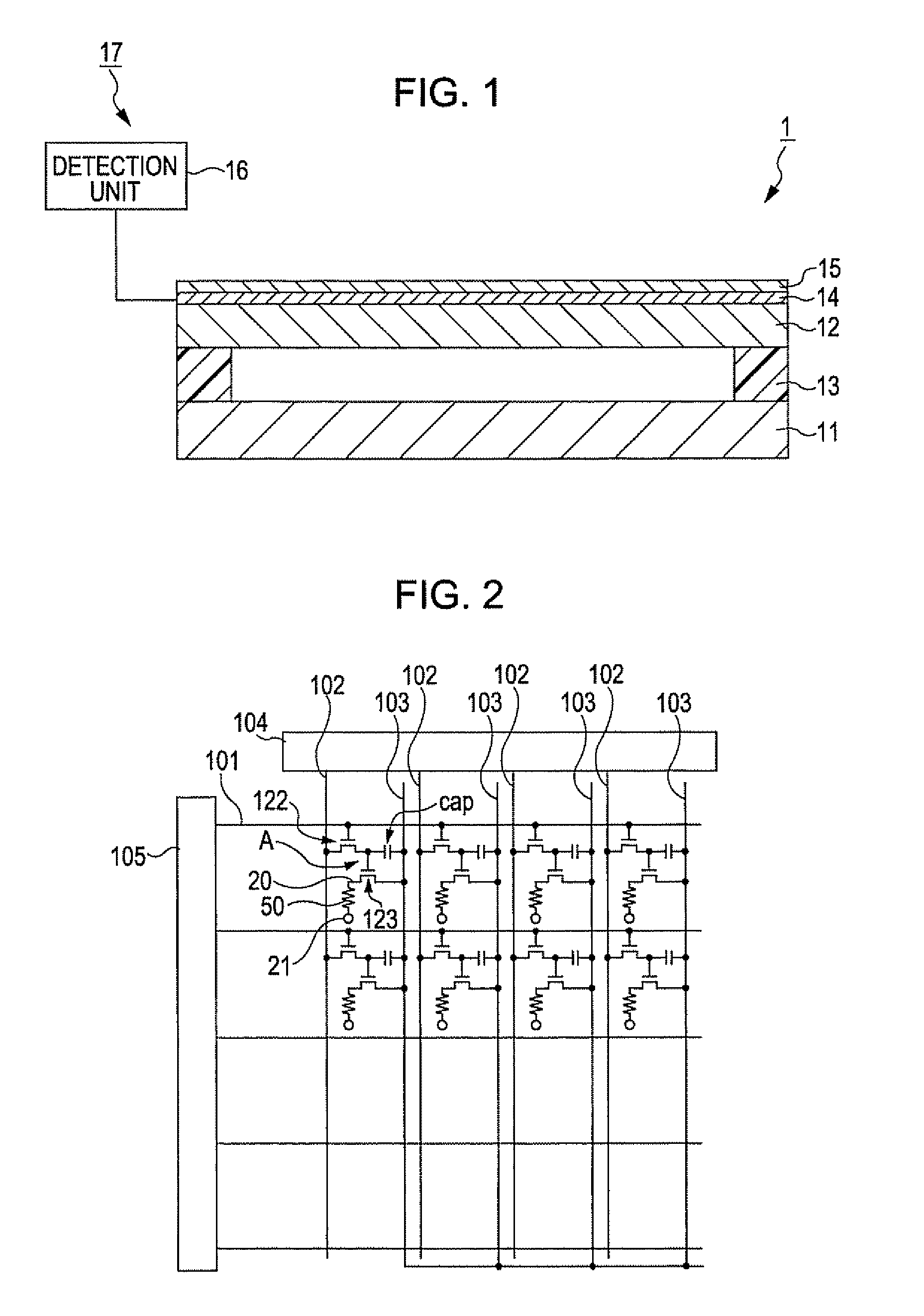
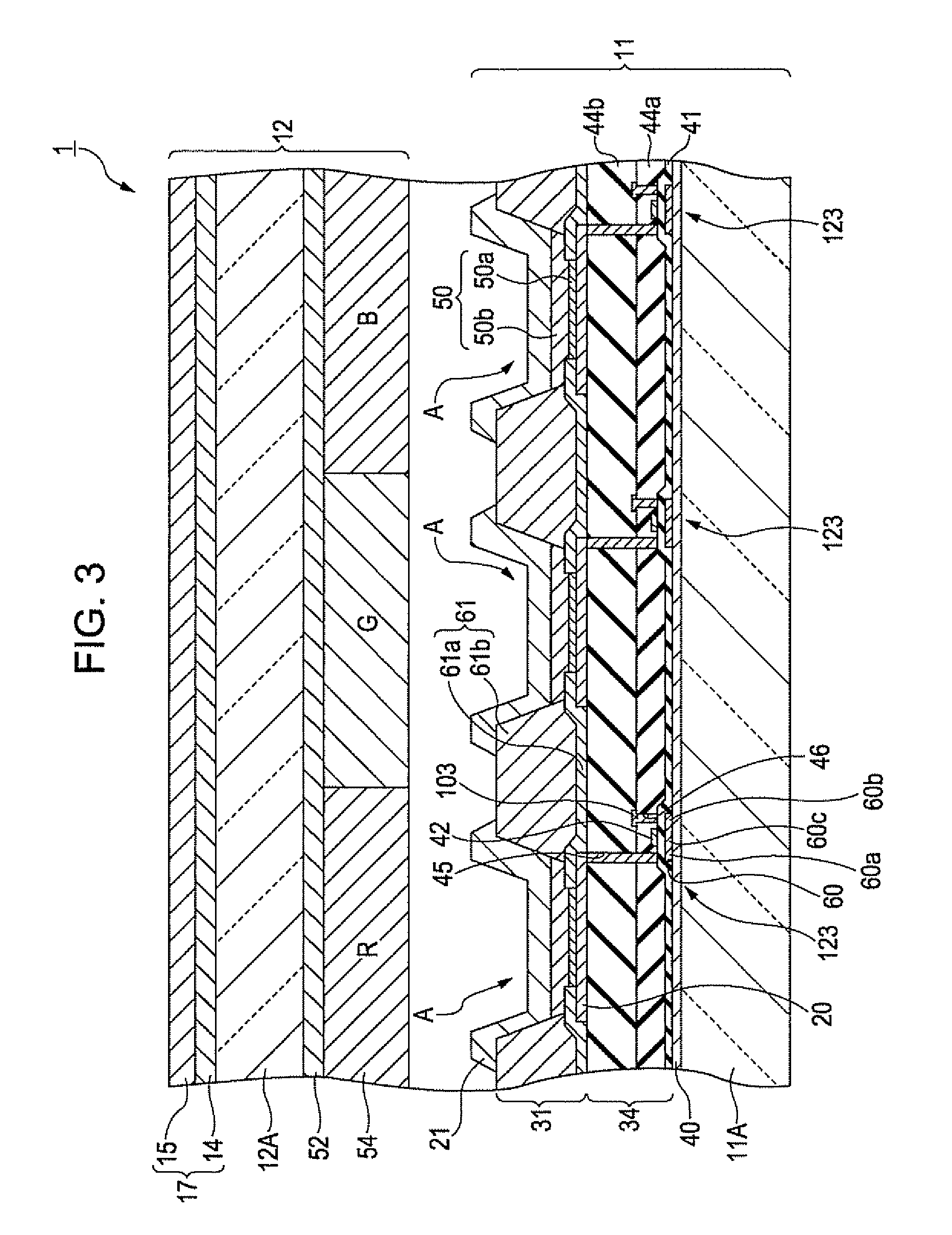
[0026]With reference to the accompanying drawings, an organic electroluminescence device having an input function according to a first exemplary embodiment of the present invention is described below. In the following description, for convenience of explanation, an “organic electroluminescence device having an input function” may be simply referred to as “organic EL device having an input function” or “touch-sensitive organic EL device”, where the term “touch-sensitive” is a non-limiting paraphrasing of “having an input function”, if the context allows. It should be noted that different scales are used for members illustrated in each of the accompanying drawings that are referred to in the following explanation so that each of the members illustrated therein has a size that is easily recognizable. FIG. 1 is a sectional view that schematically illustrates an example of the configuration of a touch-sensitive organic EL device (an organic electroluminescence device having an input func...

second embodiment

[0057]Next, with reference to the accompanying drawings, an organic EL device having an input function according to a second exemplary embodiment of the invention is explained below. FIG. 4 is a sectional view that schematically illustrates the layer configuration of sub pixel regions, An organic EL device having an input function according to the present embodiment of the invention differs from the organic EL device 1 having an input function according to the first exemplary embodiment of the invention described above only in terms of the layer configuration of sub pixel regions. That is, except for the layer configuration of sub pixel regions, an organic EL device having an input function according to the present embodiment of the invention has the same configuration as that of the organic EL device 1 having an input function according to the first exemplary embodiment of the invention. Accordingly, in the following description, an explanation is given with a focus on the differen...

third embodiment

[0060]Next, with reference to the accompanying drawings, an organic EL device having an input function according to a third exemplary embodiment of the invention is explained below. FIG. 5 is a sectional view that schematically illustrates the layer configuration of sub pixel regions. An organic EL device having an input function according to the present embodiment of the invention differs from the organic EL device 1 having an input function according to the first exemplary embodiment of the invention described above only in that, in the present embodiment of the invention, an individual light-emitting material corresponding to one of R, G, and B color components is provided in each of the sub pixel regions, thereby omitting a color filter layer. Except for the above difference, an organic EL device having an input function according to the present embodiment of the invention has the same configuration as that of the organic EL device 1 having an input function according to the fir...


PUM


Abstract

The invention provides an organic electroluminescence device having an input function, including: an element substrate that has a light-emitting layer sandwiched between a positive electrode and negative electrode in each of a plurality of sub pixel regions that are arrayed in a matrix pattern; a sealing substrate that seals the element substrate; and a touch panel section that is provided at the outer-surface side of the sealing substrate. In such a configuration of the organic electroluminescence device having an input function according to an aspect of the invention, the negative electrode is formed on an individual basis so as to correspond to the display color of each of the sub pixel regions; and the sealing substrate has a shield conductor that is formed on the element-substrate side of the sealing substrate, the shield conductor having a fixed potential.

Description

BACKGROUND[0001]1. Technical Field[0002]The present invention relates to an organic electroluminescence device that has an input function. The invention further relates to an electronic apparatus that is provided with such an organic electroluminescence device.[0003]2. Related Art[0004]These days, there are growing expectations for the exploitation of organic electroluminescence devices to a variety of applications such as full-color display use. With the increasing expectations placed thereon, technical study and development of organic electroluminescence devices are now conducted actively. An organic electroluminescence device (i.e., apparatus) uses organic electroluminescence elements as its picture elements, that is, pixels (hereafter the term “electroluminescence” is abbreviated as “EL”). Since an organic EL element is a device (i.e., element) that is driven by an electric current, any variation or fluctuation in a driving electric current supplied thereto leads directly to the...

Claims


Application Information

Patent Timeline
Patent Type & Authority Applications(United States)
IPC IPC(8): H01L51/54H01J1/62
CPCG06F3/044H01L27/323G09G3/3225H01L27/3244G06F3/0444H10K59/40H10K59/12G06F3/0412G06F3/0445
Inventor KOSHIHARA, TAKESHIUTSUNOMIYA, SUMIOUSHIKI, TAKEYOSHIFUJIKAWA, YOICHI
Owner ELEMENT CAPITAL COMMERCIAL CO PTE LTD
Why Eureka
Try Eureka