High speed semiconductor optical modulator

a high-speed semiconductor and optical modulator technology, applied in the field of communication systems, can solve the problems of uneven response of traditional devices, dc power consumption, and different requirements for activating devices

Inactive Publication Date: 2008-09-04
ALCATEL-LUCENT USA INC +1
View PDF8 Cites 35 Cited by
  • Summary
  • Abstract
  • Description
  • Claims
  • Application Information

AI Technical Summary

Benefits of technology

[0006]To address the above-discussed deficiencies of the prior art, the present invention provides an optical waveguide modulator. In one embodiment, the optical waveguide modulator includes a semiconductor planar optical waveguide core and doped semiconductor connecting paths located adjacent opposite sides of the core and capable of applying a voltage across the core, wherein the optical waveguide core and connecting paths form a structure having back-to-back PN semiconductor junctions. In another embodiment, the optical waveguide modulator includes a semiconductor optical waveguide core including a ridge portion wherein the ridge portion has at least one PN semiconductor junction located therein. The optical waveguide modulator also includes one or more doped semiconductor connecting paths located laterally adjacent the ridge portion and capable of applying a voltage to the ridge portion.

Problems solved by technology

Traditional devices also have uneven responses wherein the time required to activate the device is very different from the time required to deactivate the device.
This requires a voltage bias to be applied to the device, wherein DC power consumption results.
Response speed for these devices is also limited, since carriers have to traverse the entire distance between ohmic contacts of the device in order to activate and deactivate the device.
Additionally, current devices have severe bandwidth limitations and incur relatively large optical losses corresponding to changes in their optical refractive index.

Method used


Image

  • High speed semiconductor optical modulator
  • High speed semiconductor optical modulator
  • High speed semiconductor optical modulator

Examples


Embodiment Construction

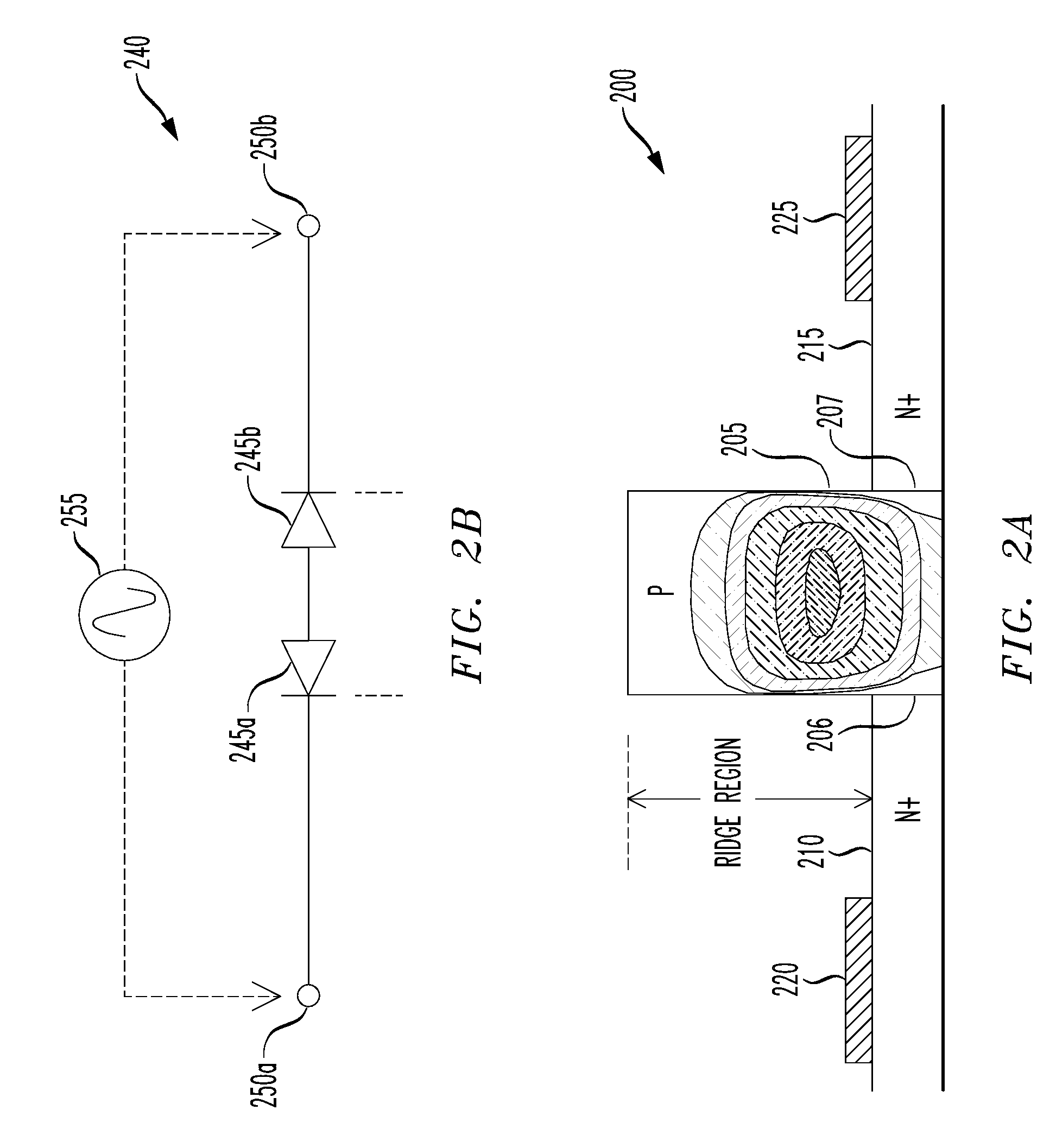
[0020]Herein, the various semiconductor structures may be fabricated from various semiconductors, e.g., silicon or compound semiconductors, by conventional micro-fabrication methods.

[0021]Herein, the various optical waveguide cores may be covered with one or more top optical cladding layers, e.g., silica glass layers.

[0022]Herein, electrodes may be fabricated of metal and or heavily doped semiconductor, e.g., doped polysilicon, by conventional micro-fabrication methods.

[0023]Herein, maximum cited concentrations of positive and negative charge carriers provide lower bounds on concentrations of respective p-type and n-type dopants in described semiconductor structures.

[0024]Embodiments of the present invention are particularly well suited for high speed, highly integrated, cost effective, large-scale applications of communication systems or subsystems. The CMOS compatibility of this design makes it appropriate for high-volume fabrication. The significant improvement in device response...


PUM

PropertyMeasurementUnit
DC bias voltageaaaaaaaaaa
voltagesaaaaaaaaaa
voltagesaaaaaaaaaa

Abstract

The present invention provides an optical waveguide modulator. In one embodiment, the optical waveguide modulator includes a semiconductor planar optical waveguide core and doped semiconductor connecting paths located adjacent opposite sides of the core and capable of applying a voltage across the core. The optical waveguide core and connecting paths form a structure having back-to-back PN semiconductor junctions. In another embodiment, the optical waveguide modulator includes a semiconductor optical waveguide core including a ridge portion wherein the ridge portion has at least one PN semiconductor junction located therein. The optical waveguide modulator also includes one or more doped semiconductor connecting paths located laterally adjacent the ridge portion and capable of applying a voltage to the ridge portion.

Description

U.S. GOVERNMENT[0001]The U.S. Government has a paid-up license in this invention and the right, in limited circumstances, to require the patent owner to license others on reasonable terms as provided for by the terms of Contract Number HR0011-05-C-0027 of DARPA.TECHNICAL FIELD OF THE INVENTION[0002]The present invention is directed, in general, to communication systems and, more specifically, to an optical waveguide modulator and a method of operating an optical waveguide.BACKGROUND OF THE INVENTION[0003]Current silicon-based (Si-based) CMOS-compatible electro-optic modulators generally have response bandwidths (i.e., 3 dB bandwidths) that are limited to a few gigahertz (GHz), at best. Traditional devices also have uneven responses wherein the time required to activate the device is very different from the time required to deactivate the device. These devices have traditionally relied on carrier injection into the optical waveguide to create effective optical refractive index change...

Claims


Application Information

Patent Timeline
Patent Type & Authority Applications(United States)
IPC IPC(8): G02F1/035
CPCG02F2001/0152G02F1/025G02F1/0152G02F1/017
Inventor GILL, DOUGLAS M.JONES, CHRISTOPHER D.W.PATEL, SANJAYRASRAS, MAHMOUDWEIMANN, NILS G.
Owner ALCATEL-LUCENT USA INC
Why Eureka
Try Eureka