Carrier for electrophotographic developer, developer, image forming method, image forming apparatus, and process cartridge
a technology for electrophotography and developer, which is applied in the field of carrier for electrophotographic developer, developer, image forming method, image forming apparatus, and process cartridge, can solve the problems of carrier that is stirred along with the toner in the developing tank deterioration, excessive rise of the developing property of the developer, and gradual decrease of carrier resistance and developer chargeability. the effect of reducing the development property of the developer and reducing the development cos
- Summary
- Abstract
- Description
- Claims
- Application Information
AI Technical Summary
Benefits of technology
Problems solved by technology
Method used
Image
Examples
manufacturing example 1
[0298]
acrylic resin solution2,130parts(solids concentration: 50 wt %)aminosilane (solids concentration: 100 wt %)4partssilica microparticles1,500parts(volumetric average diameter: 0.07 μm)toluene6,000parts
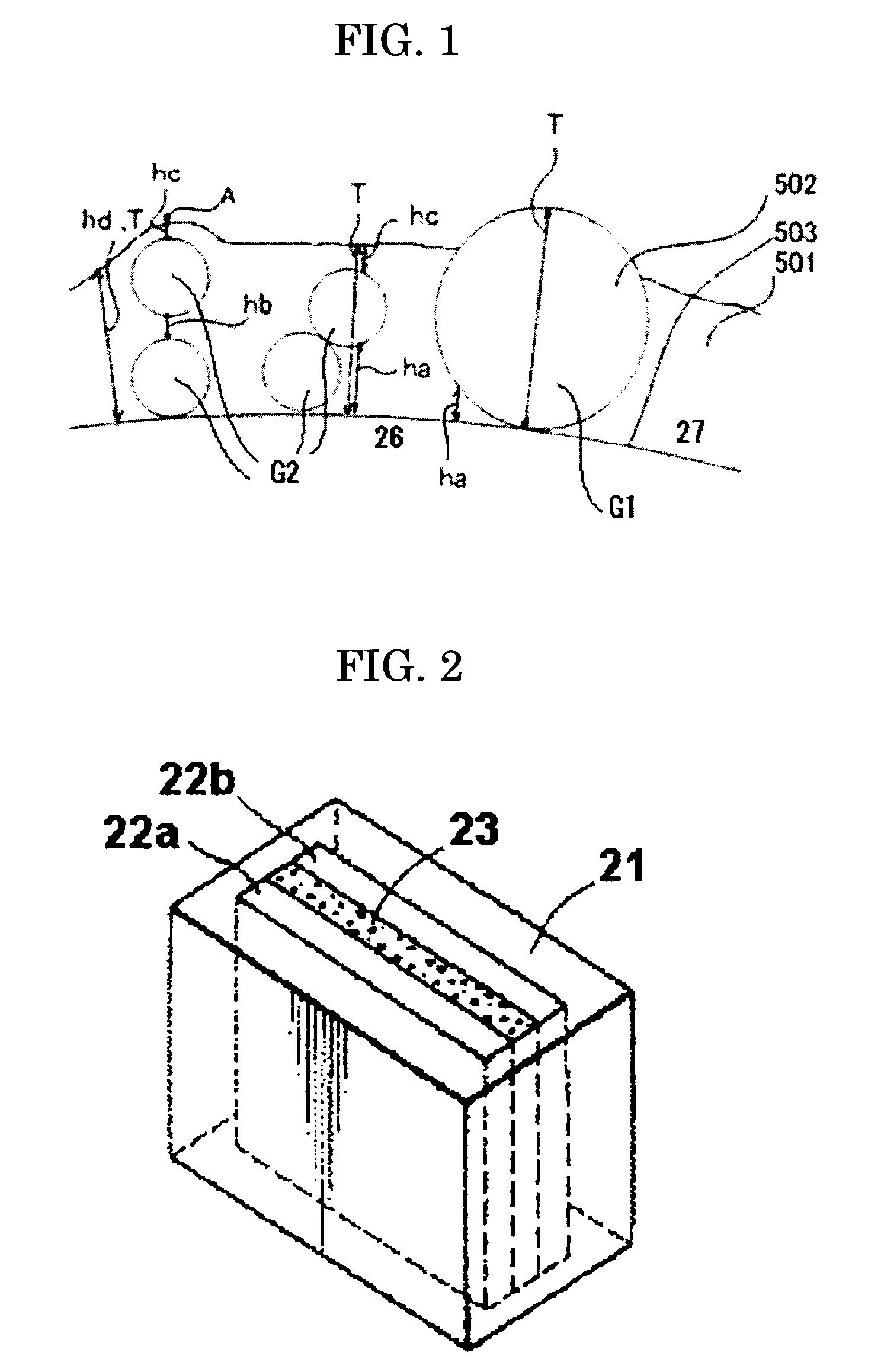
[0299]The above materials were dispersed for 10 minutes in a homomixer to prepare a resin layer formation solution. The core a in Table 1 was used as a carrier core, which was coated with the above-mentioned resin solution at a rate of 30 g / min in a 55° C. atmosphere with a spin coater (made by Okada Seiko) so that the thickness h on the core surface would be 0.15 μm, and the coating was dried. The layer thickness was adjusted by varying the amount of solution. The carrier thus obtained was baked for 1 hour at 150° C. in an electric furnace, then cooled, after which it was broken up with a sieve having a mesh of 100 μm, which gave a carrier I. The average thickness T was 0.20 μm.
[0300]The volumetric average particle diameter of the core was measured using an SRA type of Microtrac p...
manufacturing example 2
[0303]The carrier II shown in Table 2 was obtained in exactly the same manner as in Manufacturing Example 1, except that the core b shown in Table 1 was used as the carrier core. The average thickness T was 0.20 μm.
manufacturing example 3
[0304]
acrylic resin solution1,500parts(solids concentration: 50 wt %)silicone resin solution1,575parts(solids concentration: 20 wt %)aminosilane (solids concentration: 100 wt %)4partssilica microparticles1,500parts(volumetric average diameter: 0.07 μm)toluene6,000parts
[0305]A carrier III was obtained in the same manner as in Manufacturing Example 1, except that the materials of the resin layer formation solution were changed as above. The average thickness T was 0.20 μm.
PUM
 Abstract
Description
Claims
Application Information


