Memory Gate Stack Structure

a technology of memory gate and stack structure, applied in the direction of basic electric elements, electrical apparatus, semiconductor devices, etc., can solve the problem of difficult threshold voltage control after erasure, and achieve the effect of smaller conduction band offset and large valence band offs

Inactive Publication Date: 2008-09-11
NAT UNIV OF SINGAPORE
View PDF10 Cites 8 Cited by
  • Summary
  • Abstract
  • Description
  • Claims
  • Application Information

AI Technical Summary

Benefits of technology

[0038]wherein the charge storage layer comprises an amorphous material exhibiting a larger valence band offset with respect to the silicon-based material compared to Si3N4, and exhibiting a smaller conduction band offset with respect to the silicon-based material compared to Al2O3.

Problems solved by technology

Hence threshold voltage control after erasing is difficult.
If the electrical erase continues beyond a specified point, it will result in more positive charges in the silicon nitride (Si3N4) storage layer, resulting in over-erase.

Method used


Image

  • Memory Gate Stack Structure
  • Memory Gate Stack Structure
  • Memory Gate Stack Structure

Examples


Embodiment Construction

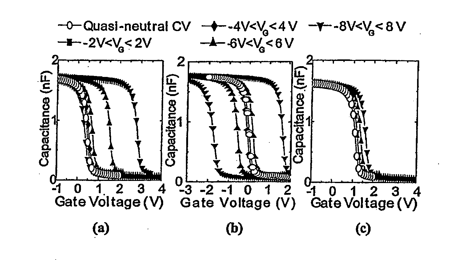
[0057]The preferred embodiment described provides a memory gate stack structure for use in a memory transistor having both an acceptable over-erase characteristic, and an acceptable charge retention capability.

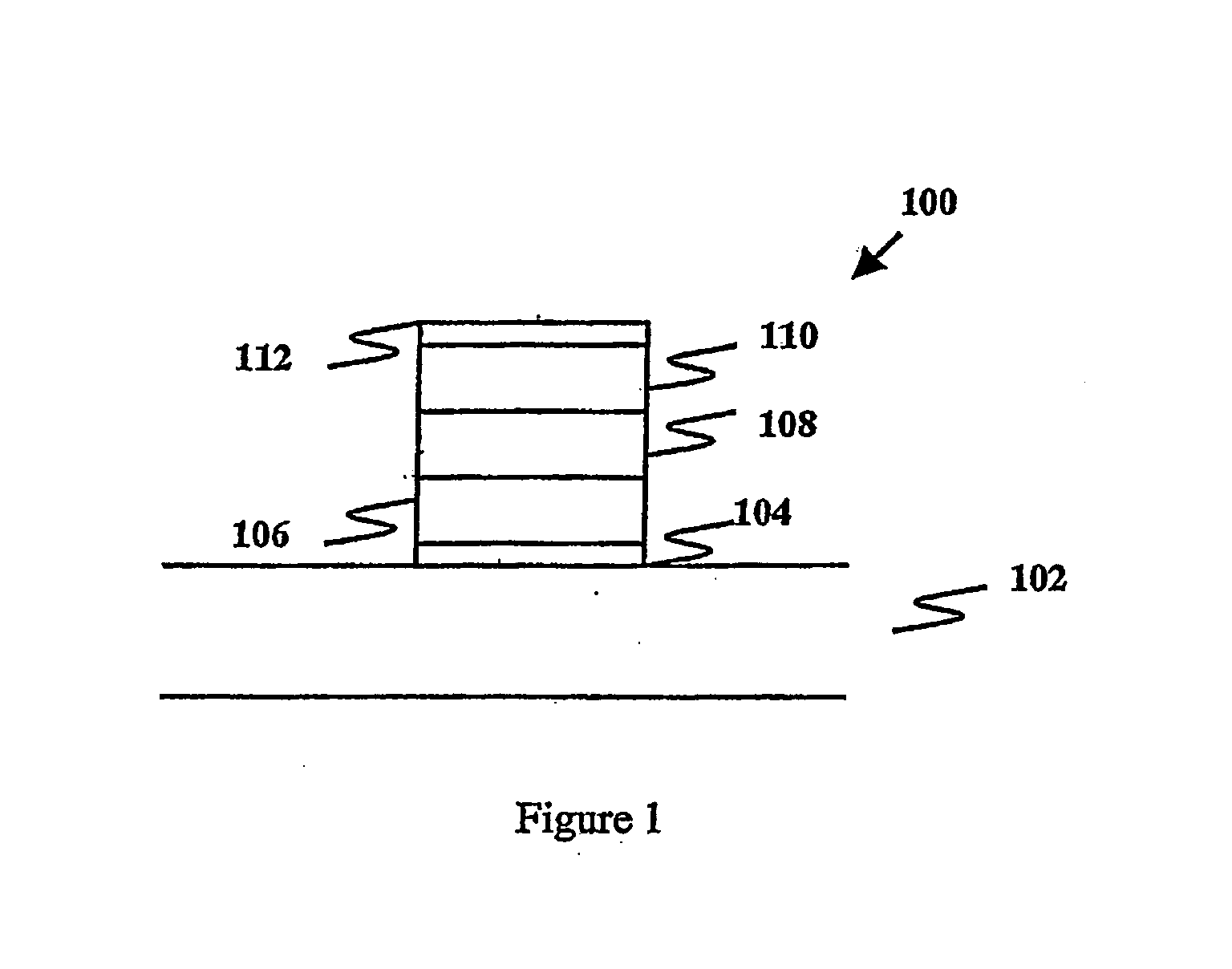
[0058]In order to obtain comparative data on the function of gate stack structures for a memory transistor, four different memory gate stack structures were fabricated and analysed. FIG. 1 is a schematic cross sectional view of the general memory gate stack structure 100, consisting of a substrate 102, a tunnel layer 104, a charge storage layer 106, a blocking layer 108, a gate layer 110, and a capping layer 112.

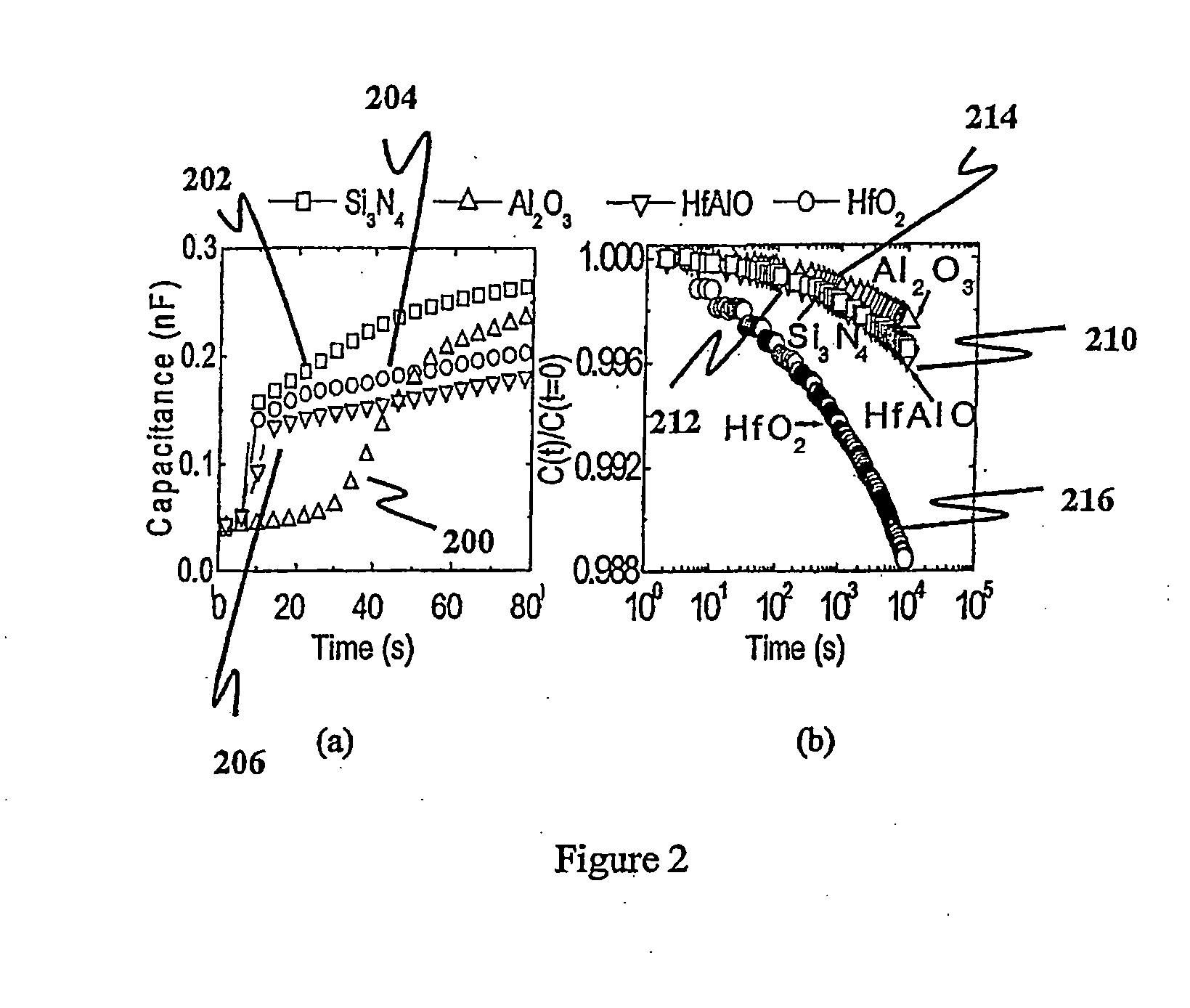
[0059]For each device, the processing conditions were the same except for the formation of the charge storage layer 106, that is, Si3N4 for a conventional MONOS device, HfO2 for a comparative device, HfAlO (or (HfO2)x(Al2O3)1-x) for a device embodying the present invention, and Al2O3 for another comparative device.

[0060]Details of the structures used in conjunction wit...


PUM


Abstract

A memory gate stack structure (100) comprising a substrate layer (102) comprising a silicon-based material, a tunnel layer (104) formed on the substrate layer, a charge storage layer (106) formed on the tunnel layer and comprising a hafnium-aluminium-oxide-based material, a blocking layer (108) formed on the charge storage layer, and a gate layer (110) formed on the blocking layer.

Description

FIELD OF INVENTION[0001]The present invention relates broadly to a memory gate stack structure, and to a method of fabricating a memory gate stack structure. The present invention will be described herein with reference to a gate stack for a memory transistor structure, however, it will be appreciated that the present invention does have broader applications. For example it may be applied in capacitor memory structures.BACKGROUND[0002]The applications of digital electronics have resulted in a demand for nonvolatile memories that are densely integrated, fast, and consume little power. The metal-oxide-nitride-oxide-semiconductor (MONOS) device is a promising candidate to replace existing forms of flash memory.[0003]The MONOS structure has better charge retention than for example a polysilicon floating-gate type memory as the charges are stored in spatially isolated deep-level traps. Hence, a single defect in the tunnel oxide will generally not cause the discharge of the memory cell.[0...

Claims


Application Information

Patent Timeline
Patent Type & Authority Applications(United States)
IPC IPC(8): H01L29/792H01L21/336H01L21/8247H01L29/51
CPCH01L21/28282H01L29/511H01L29/4234H01L29/40117
Inventor TAN, YAN NYCHIM, WAI KIMCHO, BYUNG JINCHOI, WEE KIONG
Owner NAT UNIV OF SINGAPORE
Why Eureka
Try Eureka