Superlattice gradient energy band hole barrier layer structure and infrared detector

A technology of infrared detectors and superlattice layers, applied in semiconductor devices, electrical components, circuits, etc., can solve problems affecting the optical and electrical performance of infrared detection devices, poor controllability of interface quality, and difficult beam current control, etc., to achieve The effect of large valence band offset, meeting the design requirements, and small conduction band offset

Active Publication Date: 2021-01-08
WUHAN GAOXIN TECH
View PDF5 Cites 0 Cited by
  • Summary
  • Abstract
  • Description
  • Claims
  • Application Information

AI Technical Summary

Problems solved by technology

The change of the superlattice thickness period in a short period of time will make the beam current of As more difficult to control, resulting in poor controllability of the interface quality and lower material quality, which will affect the optical and electrical properties of the infrared detection device.

Method used


Image

  • Superlattice gradient energy band hole barrier layer structure and infrared detector
  • Superlattice gradient energy band hole barrier layer structure and infrared detector

Examples


Embodiment 1

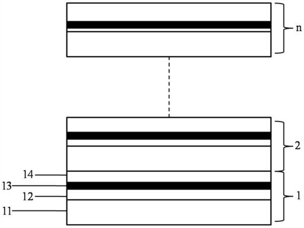
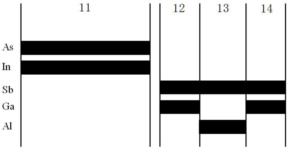
[0025] Embodiment 1: A superlattice gradient energy band hole barrier layer structure, its specific structure from bottom to top is as follows:

[0026] The first-level superlattice, with a period number of 5, is composed of 5.4nm InAs, 0.9nm GaSb, 1.5nm AlSb and 0.9nm GaSb layers, and the period thickness is 8.7nm;

[0027] The second-level superlattice, with a period number of 5, consists of 5.4nm InAs, 0.6nm GaSb, 1.5nm AlSb and 1.2nm GaSb layers, with a period thickness of 8.7nm;

[0028] The third-level superlattice, with a period number of 5, is composed of 5.4nm InAs, 0.3nm GaSb, 1.5nm AlSb and 1.5nm GaSb layers, and the period thickness is 8.7nm;

[0029] The fourth-level superlattice, with a period number of 5, consists of 5.4nm InAs, 0nm GaSb, 1.5nm AlSb and 1.8nm GaSb layers, with a period thickness of 8.7nm.

[0030] According to the analysis and calculation of the energy band theory, the energy band gap of the hole barrier layer of this structure increases from 0...

Embodiment 2

[0031] Embodiment 2: A superlattice gradient energy band hole barrier layer structure, its specific structure from bottom to top is as follows:

[0032] The first-level superlattice, with a period number of 10, is composed of 5.7nm InAs, 0.6nm GaSb, 1.8nm AlSb and 0.6nm GaSb layers, and the period thickness is 8.7nm;

[0033] The second-level superlattice, with a period of 10, consists of 5.7nm InAs, 0.3nm GaSb, 1.8nm AlSb and 0.9nm GaSb layers, with a period thickness of 8.7nm;

[0034]The third-level superlattice, with a period of 10, consists of 5.7nm InAs, 0nm GaSb, 1.8nm AlSb and 1.2nm GaSb layers, with a period thickness of 8.7nm.

[0035] According to the analysis and calculation of the energy band theory, the energy band of the hole barrier layer of this structure increases from 0.3450eV to 0.5268eV step by step from the first-level superlattice, and the corresponding conduction band offset is 0.002 eV, and the valence band offset is 0.1838eV, fully meeting the design...


PUM


Abstract

The invention relates to the technical field of hole barrier layers, and provides a superlattice gradient energy band hole barrier layer structure. The structure comprises n stages of superlattice layers, wherein each stage of superlattice layer comprises an InAs layer, a first GaSb layer, an AlSb layer and a second GaSb layer which sequentially grow from bottom to top, the period thickness of theInAs layer is A, the thickness period of the GaSb layer is C, the thickness period of the second AaSb layer is in the n-th stage of the superlattice layers, x is equal to n-1, and in each stage of the superlattice layers, the total thickness period A + B + C is equal. The invention further provides an infrared detector which comprises the superlattice gradient energy band hole barrier layer structure. By changing the insertion position, namely the position, of the AlSb layer in each stage of superlattice layer, energy band gradual change can be achieved, the thickness period of superlatticesdoes not need to be changed, the total growth time of each layer is kept unchanged, the conduction band offset of the barrier layer is small, the valence band offset is large, the design requirement of the hole barrier layer is met, structure adjustment is flexible, and epitaxial growth of materials is easy to achieve.

Description

technical field [0001] The invention relates to the technical field of hole barrier layers, in particular to a superlattice gradient energy band hole barrier layer structure and an infrared detector. Background technique [0002] The antimonide superlattice infrared detector is a research hotspot in the field of infrared detection technology in recent years. It has broad application prospects and is the preferred material for the third generation of infrared detectors. Antimonide superlattice materials have flexible energy band engineering design. Combined with molecular beam epitaxy technology, infrared detector structures that meet various needs can be grown according to the designed structure, especially InAs / GaSb II superlattice infrared detectors. . [0003] The absorption layer of a complete InAs / GaSb superlattice device structure usually consists of hundreds of periodic structures. There are problems such as stress mismatch and interface interdiffusion between InAs a...

Claims


Application Information

Patent Timeline
IPC IPC(8): H01L31/0304H01L31/0352H01L31/105
CPCH01L31/0304H01L31/035236H01L31/105
Inventor 刘永锋张传杰
Owner WUHAN GAOXIN TECH
Why Eureka
Try Eureka