Ultraviolet light emitting diode epitaxial wafer and method of making the same

A technology of light-emitting diodes and manufacturing methods, applied in semiconductor devices, electrical components, nanotechnology, etc., can solve the problems of weakened carrier confinement ability, unfavorable confinement of electrons, and low quantum efficiency in ultraviolet LEDs, so as to improve migration and improve Effects of Luminous Efficiency and Lateral Migration

Active Publication Date: 2020-10-09
HC SEMITEK SUZHOU
View PDF7 Cites 0 Cited by
  • Summary
  • Abstract
  • Description
  • Claims
  • Application Information

AI Technical Summary

Problems solved by technology

[0005] The energy band difference between GaN and AlGaN is small, which will lead to the weakening of the carrier confinement ability of the multi-quantum well layer, which will reduce the luminous efficiency of the LED
At the same time, the valence band shift of GaN / AlGaN heterojunction is relatively large (about 0.5eV), and the conduction band shift is small (about 1.4eV). The small shift is not conducive to confining electrons, which will lead to low internal quantum efficiency of UV LEDs

Method used


Image

  • Ultraviolet light emitting diode epitaxial wafer and method of making the same
  • Ultraviolet light emitting diode epitaxial wafer and method of making the same

Examples


Embodiment Construction

[0029] In order to make the object, technical solution and advantages of the present invention clearer, the implementation manner of the present invention will be further described in detail below in conjunction with the accompanying drawings.

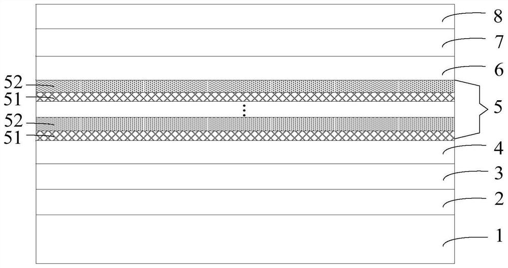
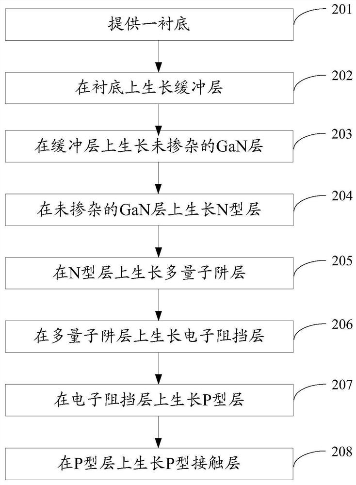
[0030] figure 1 It is a schematic structural diagram of an ultraviolet light-emitting diode epitaxial wafer provided by an embodiment of the present invention, as shown in figure 1 As shown, the ultraviolet light-emitting diode epitaxial wafer includes a substrate 1, and a buffer layer 2, an undoped GaN layer 3, an N-type layer 4, a multi-quantum well layer 5, and an electron blocking layer 6 stacked on the substrate 1 in sequence. , P-type layer 7 and P-type contact layer 8 .

[0031] The multi-quantum well layer 5 is composed of multiple periodic superlattice structures, and each superlattice structure includes GaN well layers 51 and BAlN barrier layers 52 stacked in sequence.

[0032] In the embodiment of the present invention, th...


PUM

PropertyMeasurementUnit
thicknessaaaaaaaaaa
thicknessaaaaaaaaaa
temperatureaaaaaaaaaa

Abstract

The invention discloses a UVLED (ultraviolet light emitting diode) epitaxial wafer and a manufacturing method thereof and belongs to the technical field of semiconductors. The UVLED epitaxial wafer comprises a substrate as well as a buffer layer, an undoped GaN layer, an N-type layer, a multiple quantum well layer, an electron barrier layer, a P-type layer and a P-type contact layer which are sequentially stacked on the substrate, wherein the multiple quantum well layer consists of superlattice structures with multiple cycles, and each superlattice structure comprises a GaN well layer and a BAlN barrier layer which are sequentially stacked. Compared with existing GaN / AlGaN heterojunctions, a GaN / BAlN heterojunction has smaller valence-band offset and larger conduction band offset, can better limit electrons in the GaN well layer and can improve hole migration; and a GaN / BAlN heterojunction interface has high-concentration two-dimensional electron gas, can improve the lateral transfer capability of carriers and finally improves the radiative recombination efficiency of electrons and holes, so that the light emitting efficiency of the UVLED is improved.

Description

technical field [0001] The invention relates to the technical field of semiconductors, in particular to an epitaxial wafer of an ultraviolet light emitting diode and a manufacturing method thereof. Background technique [0002] UV Light Emitting Diode (UVLED for short) is a solid-state ultraviolet light source. It has many advantages such as no pollution, small size, low energy consumption, and long life. It is widely used in medical and health (such as sterilization, cancer detection, skin disease treatment, etc.) ), environmental protection (such as the rapid decomposition of pollutants such as dioxins, polychlorinated biphenyls, and pesticides, and the purification of water and air), lighting (such as white light-emitting diodes with high color rendering index) and other fields. [0003] Epitaxial wafers are an important component in the manufacture of LEDs. The existing ultraviolet light-emitting diode epitaxial wafer includes a substrate, and an undoped GaN layer, an N...

Claims


Application Information

Patent Timeline
Patent Type & Authority Patents(China)
IPC IPC(8): H01L33/06H01L33/32H01L33/00B82Y40/00
CPCB82Y40/00H01L33/007H01L33/06H01L33/32
Inventor 刘旺平乔楠吕蒙普胡加辉李鹏
Owner HC SEMITEK SUZHOU
Why Eureka
Try Eureka