Ultraviolet led epitaxial wafer and its preparation method and application

An LED epitaxial wafer and ultraviolet technology, which is applied in the field of diodes, can solve the problems of small valence band energy level, low luminous efficiency of ultraviolet LED devices, and easy escape of electrons from the active area, so as to reduce the hole barrier height and improve the injection. Efficiency, the effect of increasing the effective barrier height

Active Publication Date: 2022-02-22
GUANGDONG INST OF SEMICON IND TECH
View PDF7 Cites 0 Cited by
  • Summary
  • Abstract
  • Description
  • Claims
  • Application Information

AI Technical Summary

Problems solved by technology

[0004] In order to solve the problem that electrons are easy to escape from the active area and holes are not easy to inject into the active area in the ultraviolet LED device, resulting in low luminous efficiency of the ultraviolet LED device, the inventor thought of improving the structure of the electron blocking layer on the ultraviolet LED epitaxial wafer, To provide a specially structured electron blocking layer with a higher conduction band energy level and a smaller valence band energy level, thereby effectively improving the radiative recombination efficiency of electrons and holes in the active region and improving the luminous efficiency of ultraviolet LED devices

Method used


Image

  • Ultraviolet led epitaxial wafer and its preparation method and application
  • Ultraviolet led epitaxial wafer and its preparation method and application
  • Ultraviolet led epitaxial wafer and its preparation method and application

Examples


Embodiment Construction

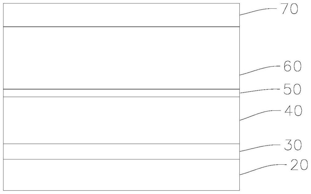
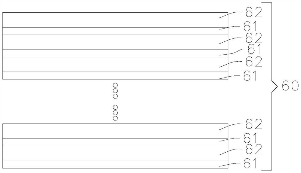
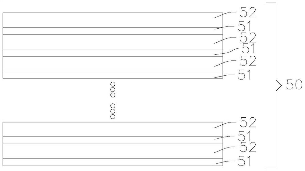
[0033] In order to make the purpose, technical solutions and advantages of the embodiments of the present invention clearer, the technical solutions in the embodiments of the present invention will be clearly and completely described below in conjunction with the drawings in the embodiments of the present invention. Obviously, the described embodiments It is a part of embodiments of the present invention, but not all embodiments. Based on the embodiments of the present invention, all other embodiments obtained by persons of ordinary skill in the art without making creative efforts belong to the protection scope of the present invention.

[0034] It should be noted that, in the case of no conflict, the embodiments in the present application and the features in the embodiments can be combined with each other.

[0035] It should also be noted that in this article, relational terms such as first and second etc. are only used to distinguish one entity or operation from another enti...


PUM

PropertyMeasurementUnit
thicknessaaaaaaaaaa
thicknessaaaaaaaaaa
thicknessaaaaaaaaaa

Abstract

The invention discloses an ultraviolet LED epitaxial sheet and its preparation method and application, wherein the ultraviolet LED epitaxial sheet includes an n-type semiconductor layer, an active layer, an electron blocking layer and a p-type semiconductor layer which are epitaxially grown in sequence; the electron blocking layer consists of a first The first sublayer and the second sublayer are alternately grown in a superlattice structure, the first sublayer is an aluminum boron nitride layer, and the second sublayer is an aluminum gallium nitride layer. The ultraviolet LED epitaxial wafer provided by the present invention uses alternately grown aluminum boron nitride layers and aluminum gallium nitride layers to form an electron blocking layer, so that the energy level position of the conduction band of the electron blocking layer is higher, and the effective barrier height of electrons is increased, effectively Block electrons from transitioning to the p-type semiconductor layer; at the same time, reduce the hole barrier height between the electron blocking layer and the active region, and significantly improve the injection efficiency of holes injected into the active layer; therefore, the radiative recombination rate of the active region can be increased, Thereby improving the luminous efficiency of the ultraviolet LED.

Description

technical field [0001] The invention relates to the technical field of diodes, in particular to an ultraviolet LED epitaxial wafer and a preparation method and application thereof. Background technique [0002] An ultraviolet light emitting diode (LED) generally includes an epitaxial wafer and electrodes prepared on the epitaxial wafer. AlGaN-based ultraviolet LED epitaxial wafers generally include: a substrate and a buffer layer, n-type semiconductor layer, active layer, electron blocking layer and p-type semiconductor layer that are epitaxially grown on the substrate in sequence. When a current is injected into the AlGaN-based ultraviolet LED, the electrons injected into the n-type semiconductor layer and the holes injected into the p-type semiconductor layer will enter the multi-quantum well active region under the action of the current and recombine to emit ultraviolet light. Among them, the electron blocking layer is generally an AlGaN electron blocking layer with a hi...

Claims


Application Information

Patent Timeline
Patent Type & Authority Patents(China)
IPC IPC(8): H01L33/14H01L33/06H01L33/00A61L2/10A61L2/26A61L9/20
CPCH01L33/145H01L33/06H01L33/0075A61L2/10A61L2/26A61L9/20A61L2202/11
Inventor 贺龙飞赵维张康何晨光吴华龙廖乾光陈志涛
Owner GUANGDONG INST OF SEMICON IND TECH
Why Eureka
Try Eureka