Method for realizing Fermi level de-pinning on surface of germanium substrate in metal- germanium contact

A Fermi level, germanium substrate technology, applied in the field of microelectronics, can solve the problems of carrier tunneling, low additional resistance, etc., and achieve small additional resistance, low conduction band offset, and good depinning effect. Effect

Inactive Publication Date: 2012-07-04
FUDAN UNIV
View PDF3 Cites 2 Cited by
  • Summary
  • Abstract
  • Description
  • Claims
  • Application Information

AI Technical Summary

Problems solved by technology

In addition, the dielectric layer used for unpinning is generally 0.5~4nm, which is easily tunneled by carriers, so it has very low additional resistance

Method used


Image

  • Method for realizing Fermi level de-pinning on surface of germanium substrate in metal- germanium contact
  • Method for realizing Fermi level de-pinning on surface of germanium substrate in metal- germanium contact
  • Method for realizing Fermi level de-pinning on surface of germanium substrate in metal- germanium contact

Examples


Embodiment Construction

[0022] The present invention is further described below by specific processing steps:

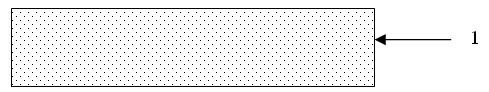
[0023] 1. Based on the n-Ge (100) substrate sheet with a resistivity of 0.05 Ω cm, rinse with HF with a concentration of 0.5%, followed by rinsing with deionized water for 5 minutes;

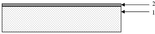
[0024] 2. Load the rinsed germanium substrate with a clean surface into the ALD cavity, and use the NH produced by the inductively coupled plasma source 3 Surface treatment of germanium substrates by plasma, chamber temperature 250°C, NH 3 Air pressure 5×10 -3 mbar, processing time 30s, radio frequency 200W, and finally form GeO of about 1nm x N y (x=0.92, y=0.08) ultra-thin dielectric layer;

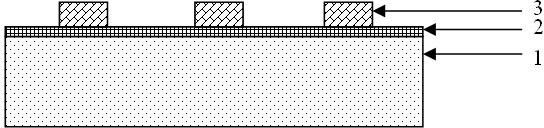
[0025] 3. With the help of a mask, use PVD technology to deposit a circular metal Al electrode with a vacuum of 10 -5 Pa, deposition power 150W, deposition time 3000s, electrode thickness 50nm, electrode diameter 500um.


PUM

PropertyMeasurementUnit
thicknessaaaaaaaaaa
thicknessaaaaaaaaaa
thicknessaaaaaaaaaa

Abstract

The invention belongs to the technical field of micro-electronics, and particularly relates to a method for realizing Fermi level de-pinning on the surface of a germanium substrate in metal- germanium contact. Germanium devices become current focuses for the advantages of high carrier mobility, realization of low equivalent oxidation layer thickness, high compatibility with existing processes and the like, but the serious surface Fermi level pinning effect of germanium is one of the problems which restrain the preparation of high-performance germanium-based N-type metal-oxide semiconductor (MOS) devices. According to the method for realizing Fermi level de-pinning on the surface of the germanium substrate in metal-germanium contact, a GeOxNy (x=0.92, y=0.08) medium layer is formed on the surface through the method of treating the germanium substrate with ammonia (NH3) plasma, so that the de-pinning effect is successfully realized; and in addition, due to the deviation of a smaller amount of energy of GeON and Ge, a prepared metal/GeON/Ge sample has lower contact resistance, and thus has higher application value.

Description

technical field [0001] The invention belongs to the technical field of microelectronics, and in particular relates to a method for realizing unpinning of the Fermi energy level on the surface of a germanium substrate when a metal is in contact with a germanium substrate. Background technique [0002] Today's semiconductor devices are constantly progressing in the direction of high efficiency and miniaturization, and CMOS devices, which are the pillars of the semiconductor industry, are developing rapidly along the direction of Moore's Law. Due to the limitations of physical limits and economic costs, devices based on traditional silicon have faced severe challenges, and new structures and materials have become the focus of research on semiconductor devices. [0003] For germanium, which is the fourth main group element with silicon, compared with silicon devices, germanium devices have higher carrier mobility and can achieve a smaller equivalent oxide layer thickness, and co...

Claims


Application Information

Patent Timeline
Patent Type & Authority Applications(China)
IPC IPC(8): H01L21/336
Inventor 蒋玉龙于浩谢琦茹国平屈新萍李炳宗张卫
Owner FUDAN UNIV
Why Eureka
Try Eureka