Programmable logic device having redundancy with logic element granularity

a logic element and logic element technology, applied in the field of programmable logic devices, can solve the problems of inability of original equipment manufacturers (oems) to design and use asics, increase design costs, and complexity, and achieve the effect of reducing the cost of design and development, and reducing the cost of developmen

Active Publication Date: 2008-09-11
TAHOE RES LTD
View PDF13 Cites 6 Cited by
  • Summary
  • Abstract
  • Description
  • Claims
  • Application Information

AI Technical Summary

Problems solved by technology

Due to the advances of chip manufacturing technology, application specific integrated circuits (ASICs) designs have become incredibly complex.
This complexity not only adds to design costs, but also the duration of time needed to develop an application specific design.
As a result, it is often not feasible for original equipment manufacturers (OEMs) to design and use ASICs.
There are several issues associated with using redundancy on a PLD.
One issue is the added cost of adding the redundant logic, which occupies space on the die, but is not available for implementing the user's circuit design.
A second issue involves connectivity.
Since each LAB row includes a relatively large number of logic elements and other circuitry, a redundancy scheme having a row granularity of a LAB represents a fairly significant penalty with regard to the overall amount of logic available on the chip.
Row granularity of one LAB also creates an interconnect issue.
Extending the length of inter-LAB lines by one LAB also creates propagation delays, particularly when staggered inter-LAB lines are used.

Method used


Image

  • Programmable logic device having redundancy with logic element granularity
  • Programmable logic device having redundancy with logic element granularity
  • Programmable logic device having redundancy with logic element granularity

Examples


Embodiment Construction

[0022]The present invention will now be described in detail with reference to a various embodiments thereof as illustrated in the accompanying drawings. In the following description, specific details are set forth in order to provide a thorough understanding of the present invention. It will be apparent, however, to one skilled in the art, that the present invention may be practiced without using some of the implementation details set forth herein. It should also be understood that well known operations have not been described in detail in order to not unnecessarily obscure the present invention. Further, it should be noted that the techniques of the present invention could be applied to a variety of systems or electronic devices such as programmable devices and application-specific integrated circuit (ASIC) devices.

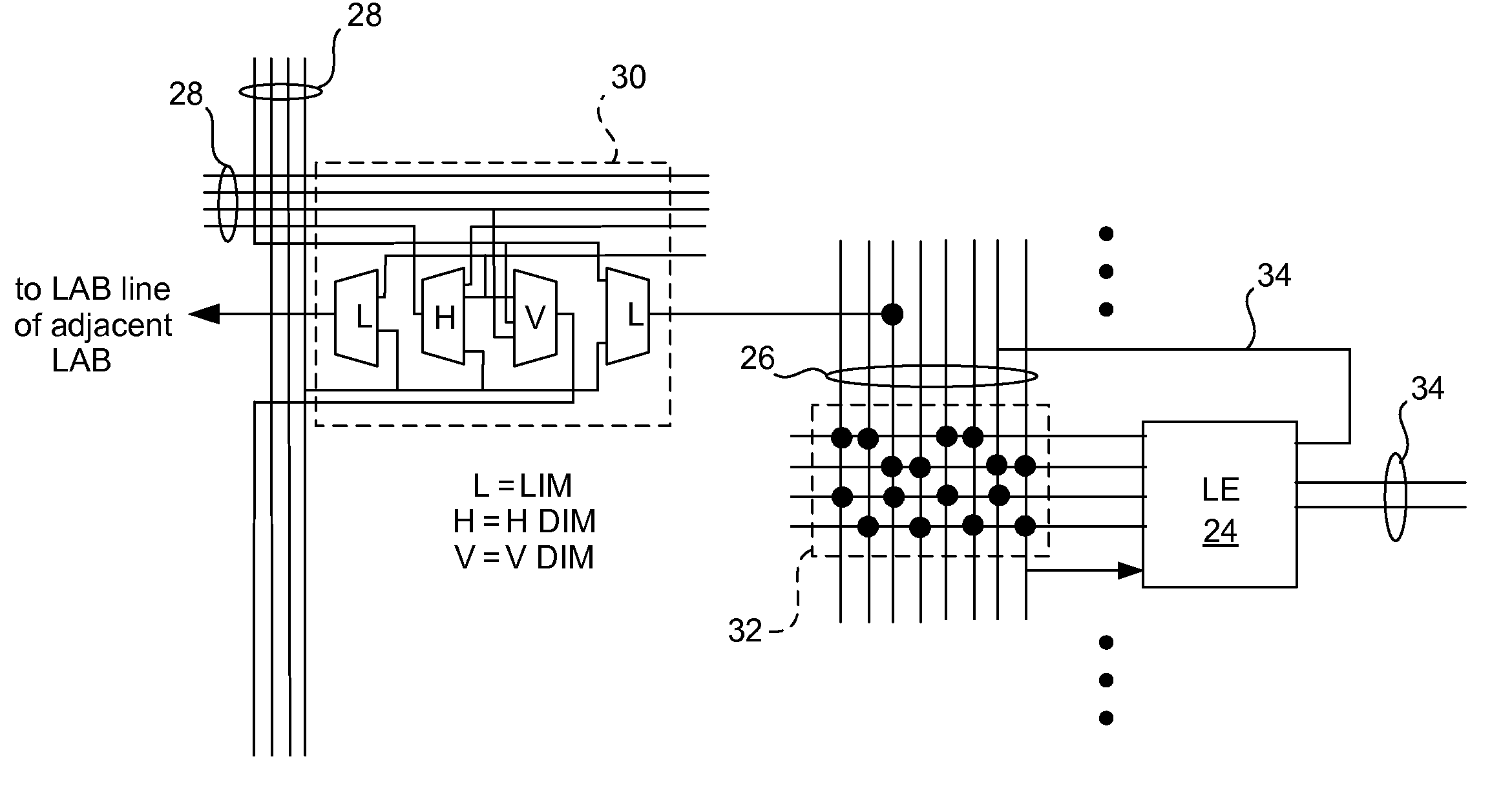
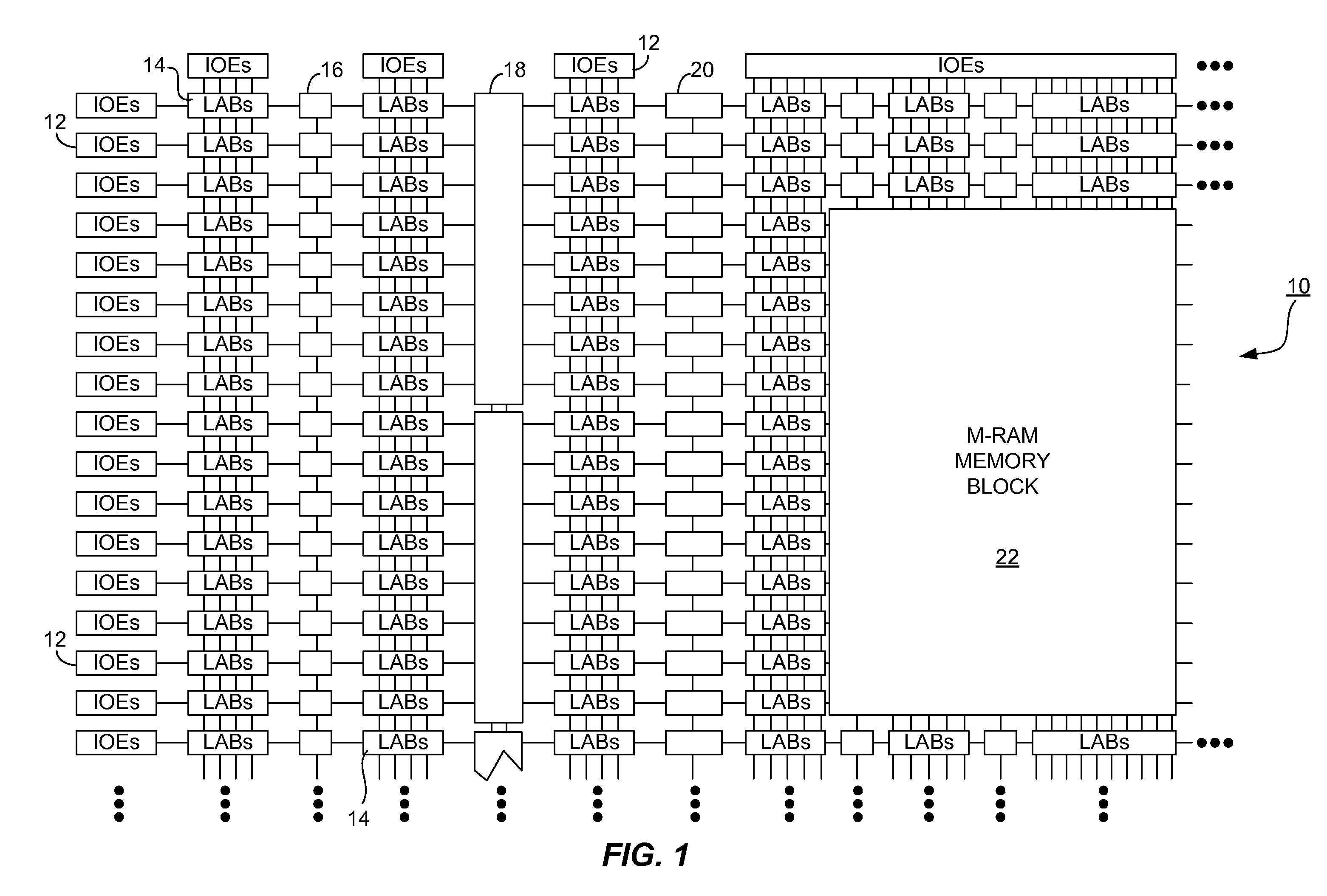
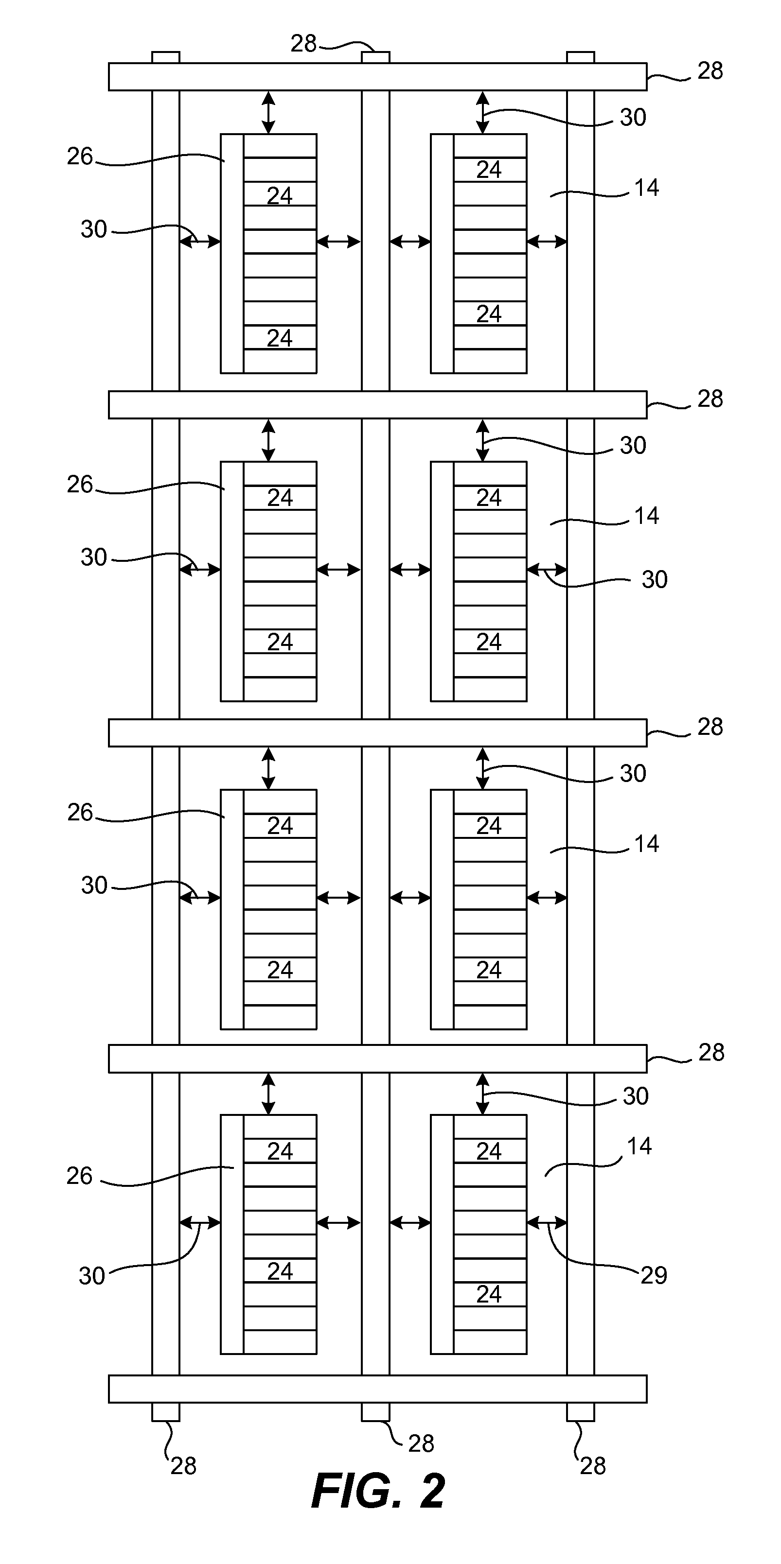
[0023]Referring to FIG. 1, a block diagram of a Programmable Logic Device (PLD) of the present invention is shown. The PLD 10 includes a two dimensional row and column b...


PUM


Abstract

A PLD having logic element row granularity redundancy is disclosed. The PLD includes a plurality of LABs arranged in an array and a plurality of horizontal and vertical inter-LAB lines interconnecting the LABs of the array. Each of the LABs further includes a predetermined number of logic elements and redundancy circuitry to replace a defective logic element with a non-defective logic element among the predetermined logic elements by shifting programming data intended to for the defective logic element to the non-defective logic element.

Description

CROSS-REFERENCE TO RELATED APPLICATIONS[0001]This application is a Continuation-in-Part of U.S. patent application Ser. No. 11 / 684,424, filed Mar. 9, 2007, and entitled “A PROGRAMMABLE LOGIC DEVICE HAVING LOGIC ARRAY BLOCK INTERCONNECT LINES THAT CAN INTERCONNECT LOGIC ELEMENTS IN DIFFERENT LOGIC BLOCKS” [Attorney Docket No.: ALTRP227 / A02527], which is hereby incorporated by reference herein.BACKGROUND[0002]1. Field of the Invention[0003]The present invention generally relates to Programmable Logic Devices (PLDs) having an array of Logic Array Blocks, each including a plurality of logic elements, and more particularly, to a PLD having redundancy with logic element granularity.[0004]2. Description of Related Art[0005]A Programmable Logic Device (PLD) is a semiconductor integrated circuit that contains fixed logic circuitry that can be programmed to perform a host of logic functions. In the semiconductor industry, PLDs are becoming increasingly popular for a number of reasons. Due to ...

Claims


Application Information

Patent Timeline
Patent Type & Authority Applications(United States)
IPC IPC(8): H03K19/177
CPCH03K19/00392H03K19/17764H03K19/17728
Inventor LEWIS, DAVIDCASHMAN, DAVID
Owner TAHOE RES LTD
Why Eureka
Try Eureka