Protection of integrated electronic circuits from electrostatic discharge

a technology electrostatic discharge, applied in emergency protective arrangements for limiting excess voltage/current, emergency protective arrangements for automatic disconnection, electrical equipment, etc., can solve problems such as circuit damage, reliability of integrated electronic circuits, and level of integration, and achieve the effect of improving the protection of electronic circuits

Active Publication Date: 2008-09-11
STMICROELECTRONICS SRL
View PDF8 Cites 2 Cited by
  • Summary
  • Abstract
  • Description
  • Claims
  • Application Information

AI Technical Summary

Benefits of technology

[0018]One embodiment improves the protection of electronic circuits from CDM stress, meaning from the electrical stresses applied during a CDM test.

Problems solved by technology

The CDM tests themselves pose a problem regarding integrated electronic circuit reliability, which is accentuated by the reduction of the characteristic sizes of MOS transistors and the corresponding increase in the level of integration.
This CDM stress can result in damage to the circuit.
In particular, CDM stress can result in short circuits or conversely in open circuits in the gate oxide layers of MOS transistors, in other irreversible deterioration, and in leakage currents.
Even so, many components do not withstand the phases of the ESD sensitivity test because of irreversible damage arising from the CDM stress.
This charge is known as the plasma charge and is the origin of later failures.

Method used


Image

  • Protection of integrated electronic circuits from electrostatic discharge
  • Protection of integrated electronic circuits from electrostatic discharge
  • Protection of integrated electronic circuits from electrostatic discharge

Examples


Embodiment Construction

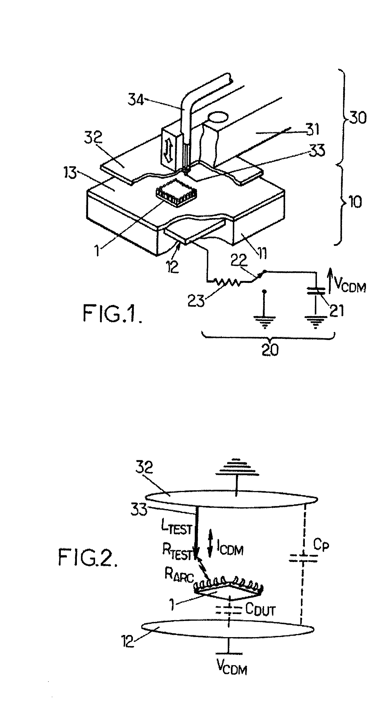
[0045]Unlike conventional ESD sensitivity test models, in which the modeled electrostatic discharge is from the testing apparatus towards the integrated circuit being tested, the charged device model or CDM represents the discharge from an integrated circuit. It is possible for components to become charged by triboelectricity, so the composition of the components (packages, size of chip and internal capacitance) is ideally taken into account in the CDM.

[0046]As shown in FIG. 1, a FCDM (“Field CDM”) test device comprises an immobile charging assembly 10, to which a charging device 20 is coupled, as well as a discharging assembly 30 which is mobile relative to the charging assembly.

[0047]The charging assembly 10 comprises a support 11, a plate forming the charging electrode 12, covered by insulation 13 (FR-4), with the electrode 12 and the insulation 13 being solidly attached to the support 11.

[0048]The charging device 20 comprises a high voltage source 21 which delivers a high CDM vo...


PUM


Abstract

Circuit nodes are identified which, in unpowered mode, can be charged with positive or negative charges but cannot be discharged. Then protective elements are added to allow the discharge of these nodes. These elements do not affect the operation of the circuit in powered mode. Discharges of the two polarities are handled, positive and negative. The circuit is thus more resistant to ESD and passes CDM tests.

Description

BACKGROUND[0001]1. Technical Field[0002]The invention relates to the protection of integrated electronic circuits from ESD (Electrostatic Discharge).[0003]It relates in general to the design of integrated electronic circuits, and more particularly to the tests used to assist with circuit design, particularly ESD sensitivity tests.[0004]2. Description of the Related Art[0005]These tests are intended to evaluate the robustness of integrated electronic circuits when they are exposed to electrostatic discharge, and to find design rules to limit the stresses related to such electrostatic discharge.[0006]For determining the sensitivity of integrated electronic circuits to electrostatic discharge, there are standardized models representing the hostile environment in which these circuits live. These models are used during the testing phase in particular to assist with the electronic circuit design.[0007]Electrostatic discharges can be so modeled using the Charged Device Model or CDM. The CD...

Claims


Application Information

Patent Timeline
Patent Type & Authority Applications(United States)
IPC IPC(8): H02H9/00H01L21/8234
CPCH01L27/0255H01L2924/0002H01L2924/00
Inventor GALY, PHILIPPEMICHELI, LAURENTTROUSSIER, GHISLAINRIEN, MICKAELVENIANT, JEAN-FRANCOIS
Owner STMICROELECTRONICS SRL
Why Eureka
Try Eureka