Spontaneous emission of telecommunication wavelength emitters coupled to at least one resonant cavity

a technology of telecommunication wavelength and emitter, which is applied in the direction of lasers, semiconductor devices, semiconductor lasers, etc., can solve the problems of not providing suitable solutions to overcome such hurdles and many different hurdles to be utilized by such devices

Inactive Publication Date: 2008-09-18
THE TRUSTEES OF COLUMBIA UNIV IN THE CITY OF NEW YORK
View PDF1 Cites 42 Cited by
  • Summary
  • Abstract
  • Description
  • Claims
  • Application Information

AI Technical Summary

Benefits of technology

[0004]The present invention relates to devices that include a structure having at least one resonant cavity and at least one emitter having an emission frequency that is substantially in the telecommunication wavelengths, where the emission frequency can be coupled to the resonant frequency of a resonant cavity so that emitted wavelengths corresponding to the resonant wavelengths of the resonant cavity are enhanced. Moreover, the devices of the present invention may be capable of operating at room temperatures.

Problems solved by technology

However, numerous different hurdles must be overcome before such devices can be utilized in practical applications.
To date, however, none of the devices provide suitable solutions to overcome such hurdles.

Method used


Image

  • Spontaneous emission of telecommunication wavelength emitters coupled to at least one resonant cavity
  • Spontaneous emission of telecommunication wavelength emitters coupled to at least one resonant cavity
  • Spontaneous emission of telecommunication wavelength emitters coupled to at least one resonant cavity

Examples


example

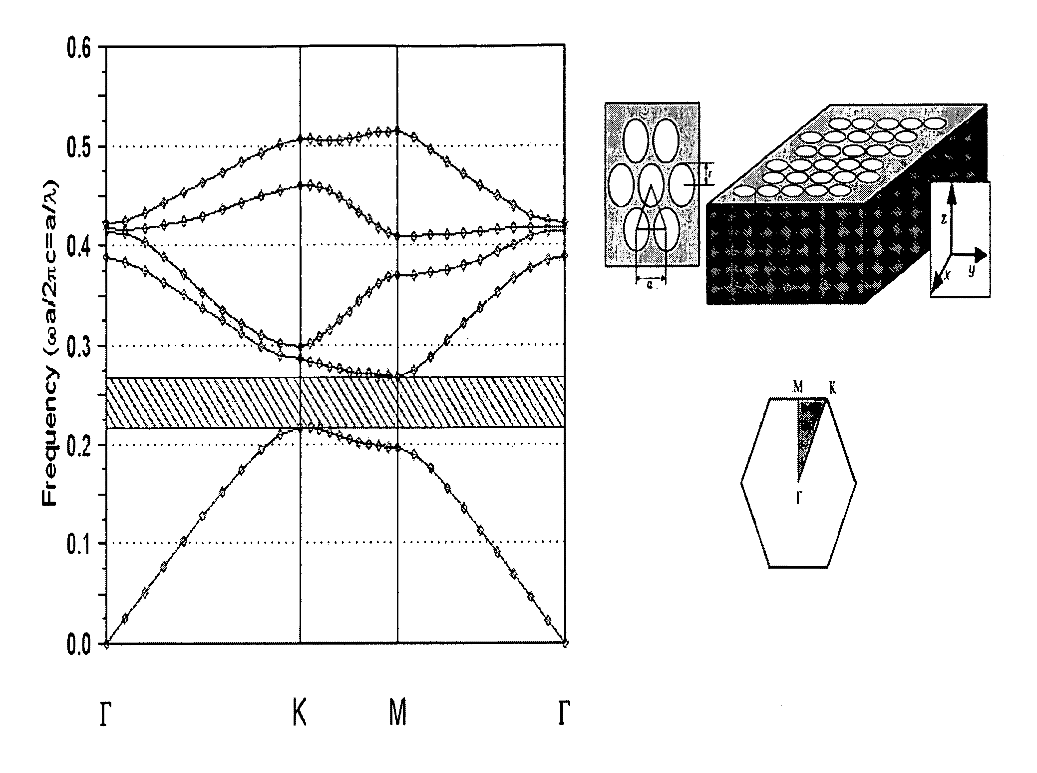
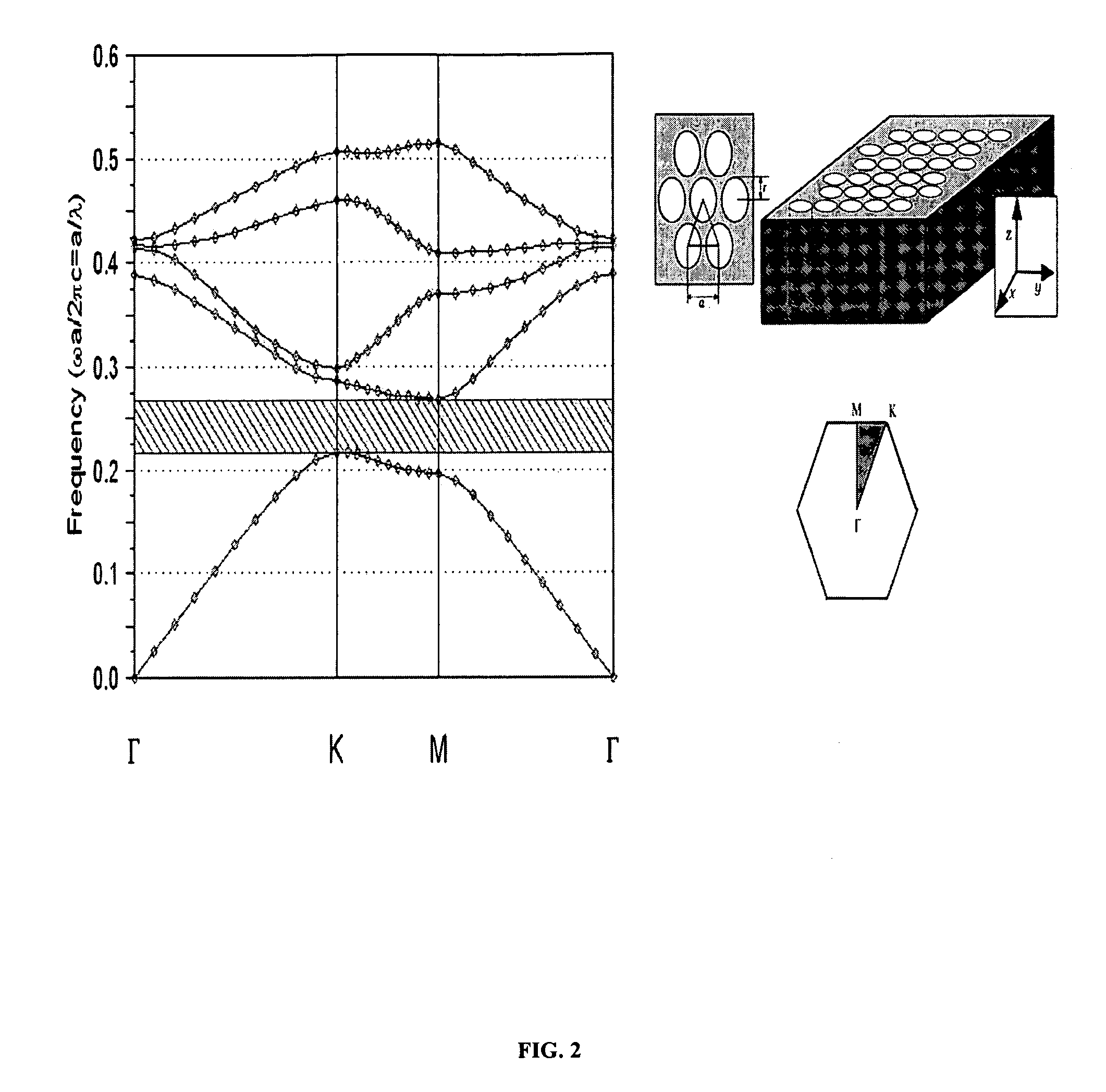
[0104]L3 nanocavities in silicon, where three air cylinders are replaced with a center cylinder (see FIG. 16), are used for studying both mid-cavity-plane and evanescent coupling of PbS quantum dots (QD). The design parameters are as follows: a=420 nm, r=0.29a (±10%), rc=0.28a (±10%), and t=0.6a, where a, r, rc, and t represent the lattice parameter, radius of holes, radius of the center hole, and slab thickness, respectively (rc=0.26a (±10%) was also used). All cavities are s1 or s3 detuned (see Akahane et al. Opt. Express, 13, p. 1202 (2005), which is incorporated by reference herein in its entirety). S1 detuning refers to lateral displacement of the air cylinders (2 total) that are near the resonant cavity and s3 detuning refers to later displacement of the 3 air cylinders (6 total) near the resonant cavity.

[0105]The silicon photonic crystal devices are fabricated on a SiO2 cladding and incorporate one or more waveguides (see FIG. 16) that allow for lensed optical fiber-waveguide...


PUM


Abstract

Systems and methods for devices that include a structure having at least one resonant cavity and at least one emitter having an emission frequency that is substantially in the telecommunication wavelengths are provided. The emission frequency can be coupled to the resonant frequency of resonant cavity so that emitted wavelengths corresponding to the resonant wavelengths of the resonant cavity are enhanced. Moreover, the devices of the present invention may be capable of operating at room temperatures.

Description

CROSS-REFERENCE(S) TO RELATED APPLICATIONS[0001]The present application claims the benefit of U.S. Patent Application No. 60 / 707,598, filed on Aug. 12, 2005, and PCT Application No. PCT / US06 / 031637, filed on Aug. 14, 2006, the contents of which are hereby incorporated by reference herein in their entireties.FIELD OF THE INVENTION[0002]The present invention relates to spontaneous emission of photons in certain structures. More particularly, the present invention relates to emitters spontaneously emitting photons that are coupled with resonant cavity structures.BACKGROUND OF THE INVENTION[0003]Control of photons has been an active area of research recently due to their numerous potential applications ranging from quantum computing, lasers, and telecommunications. However, numerous different hurdles must be overcome before such devices can be utilized in practical applications. For example, the ability operate in industry-standard wavelength ranges, the ability to fabricate such device...

Claims


Application Information

Patent Timeline
Patent Type & Authority Applications(United States)
IPC IPC(8): H01L33/00
CPCB82Y20/00H01S5/347H01S5/3412H01S5/105H01S5/11
Inventor BOSE, RANOJOYWONG, CHEE WEIGAO, JIE
Owner THE TRUSTEES OF COLUMBIA UNIV IN THE CITY OF NEW YORK
Why Eureka
Try Eureka