Structure for controlled collapse chip connection with displaced captured pads

Inactive Publication Date: 2008-09-25
IBM CORP
View PDF13 Cites 7 Cited by
  • Summary
  • Abstract
  • Description
  • Claims
  • Application Information

AI Technical Summary

Benefits of technology

[0012]As a result of the summarized invention, a solution is technically achieved in which solder attach between an IC chip and a carrier employing controlled-collapse chip connection (C4) is enhanced by allev

Problems solved by technology

However, despite the widespread use of C4 technology, implementations of new lead free solder bump alloys, BLM and chip circuitry designs have resulted i

Method used


Image

  • Structure for controlled collapse chip connection with displaced captured pads
  • Structure for controlled collapse chip connection with displaced captured pads
  • Structure for controlled collapse chip connection with displaced captured pads

Examples


Example

[0023]The detailed description explains the preferred embodiments of the invention, together with advantages and features, by way of example with reference to the drawings.

DETAILED DESCRIPTION OF SPECIFIC EMBODIMENTS

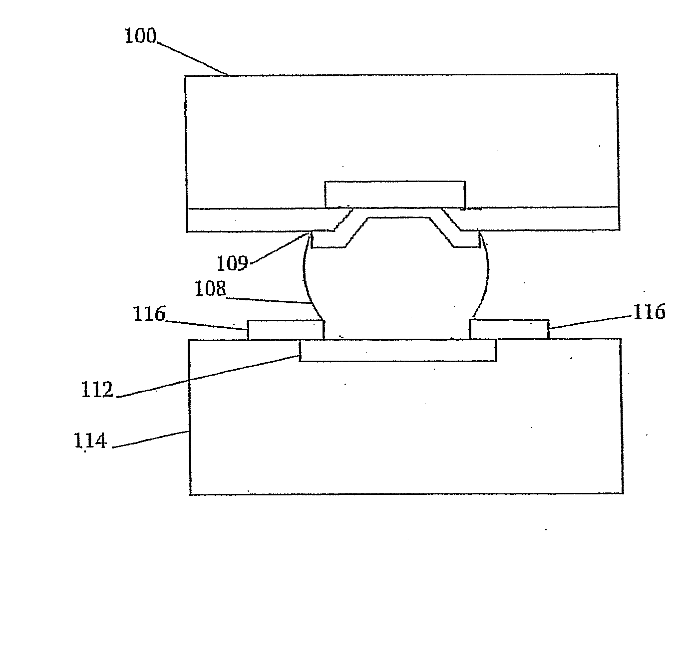
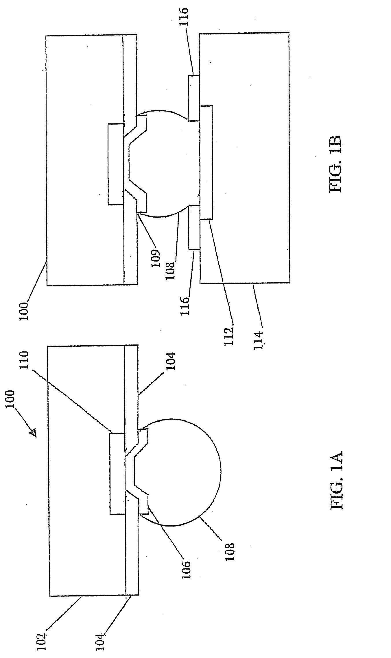
[0024]Embodiments of the present invention provide a structure and method for solder attach between an IC chip and a carrier employing controlled-collapse chip connection (C4) that is enhanced by alleviating the adverse effects resulting from stresses induced by differences in chip to carrier coefficient of thermal expansion (CTE) by varying substrate SM pad locations relative the IC chip ball limiting metallurgy (BLM). The resultant azimuthal (rotational) stretching acts to increase the compliancy of the solder connections.

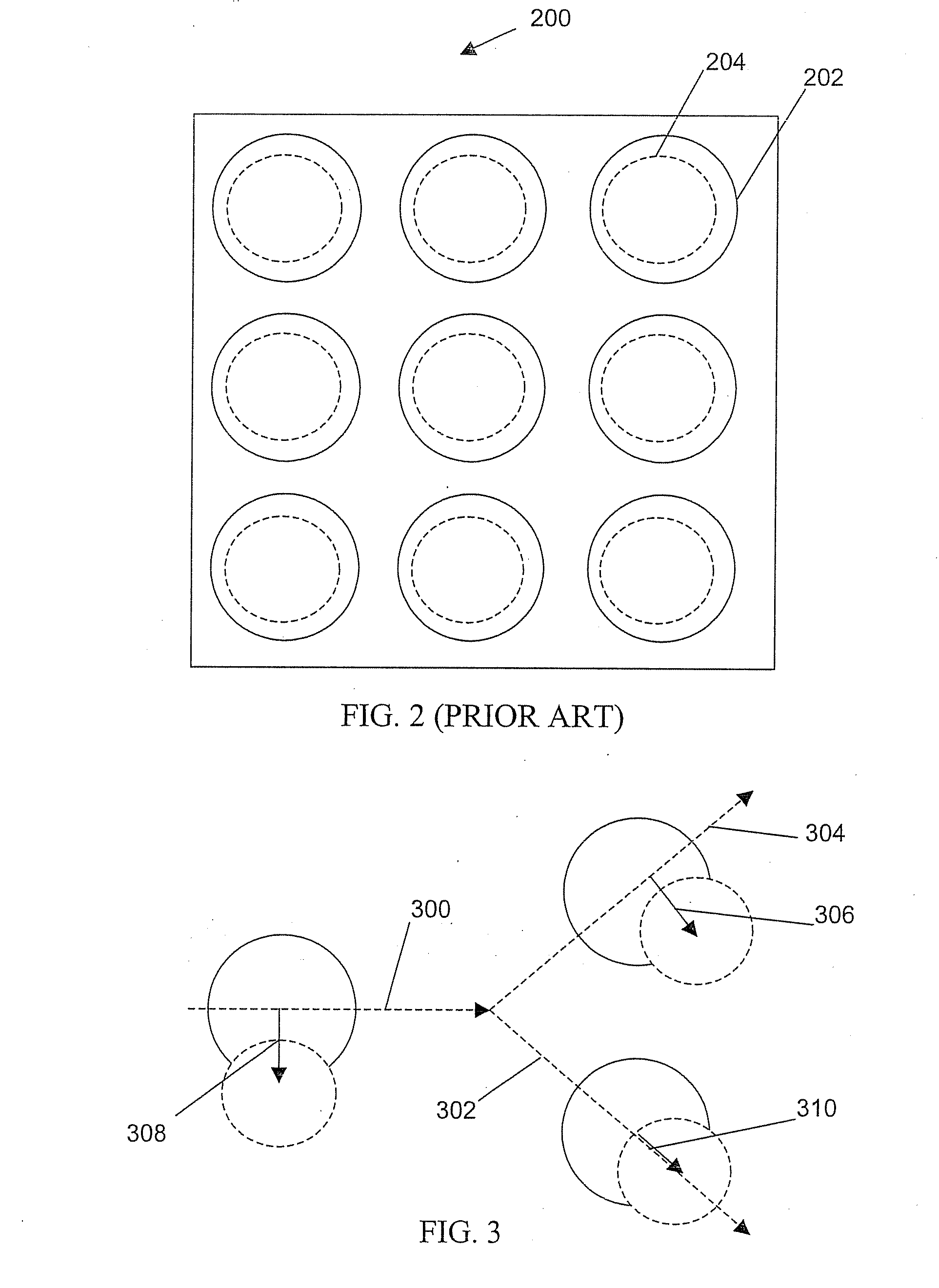
[0025]FIG. 2 is a prior art aligned ball grid array 200 that employs C4 technology to attach an IC chip to a substrate. The substrate SM pads 202 are aligned and centered to the BLM 204 (dotted lines). While it is typical for the pads and BLM to be al...


PUM


Abstract

A structure, for controlled collapse chip connection (C4) between an integrated circuit (IC) and a substrate, that alleviates the adverse effects resulting from induced stresses in C4 solder joints, the structure includes: a first and second array defined on the ball limiting metallurgy (BLM) side of the IC; a first and second array of surface mount (SM) pads arranged on the substrate placement side; and wherein the reduction of the adverse effects resulting from the induced stress in the solder joints is facilitated by varying the relative alignment of the first and second arrays of SM pads to the first and second arrays of solder balls.

Description

TRADEMARKS[0001]IBM® is a registered trademark of International Business Machines Corporation, Armonk, N.Y., U.S.A. Other names used herein may be registered trademarks, trademarks or product names of International Business Machines Corporation or other companies.BACKGROUND OF THE INVENTION[0002]1. Field of the Invention[0003]This invention relates generally to controlled collapse chip connection, and more particularly to providing a structure and method for stress reduction in solder ball attachment joints by varying alignments of solder pads in the azimuthal direction.[0004]2. Description of the Background[0005]Controlled-Collapse Chip Connection (C4) is a means of connecting IC (integrated circuit) chips to substrates in electronic packages. C4 is known as a flip-chip technology, in which the interconnections are small solder balls on the bottom side chip surface. C4 technology represents one of the highest density schemes known in the art for chip interconnections. The C4 techno...

Claims


Application Information

Patent Timeline
IPC IPC(8): H01L23/48H01L21/44
CPCH01L23/49816H01L2224/16104H01L24/02H01L24/16H01L24/17H01L2224/0401H01L2224/13099H01L2224/16H01L2924/01014H01L2924/0105H01L2924/01082H01L2924/014H01L2924/14H05K3/3436H05K2201/09427H01L2924/01006H01L2924/01033H01L2924/01043H01L2224/171H01L23/49838H01L2224/17104Y02P70/50
Inventor DUCHESNE, ERICSYLVESTRE, JULIEN
Owner IBM CORP
Why Eureka
Try Eureka