Polishing composition and polishing method

a technology of composition and polishing method, applied in the direction of lapping machine, tableware, other chemical processes, etc., can solve the problems of reducing working efficiency and reducing safety of conventional polishing composition, and achieve the effect of polishing titanium materials and high stock removal ra

Active Publication Date: 2008-09-25
FUJIMI INCORPORATED
View PDF33 Cites 4 Cited by
  • Summary
  • Abstract
  • Description
  • Claims
  • Application Information

AI Technical Summary

Benefits of technology

[0005]Accordingly, an object of the present invention is to provide a polishing composition having the ability to polish a titanium material at a high stock removal rate, and to provide a polishing method using such a polishing composition.

Problems solved by technology

However, conventional polishing compositions do not have the ability to polish a barrier layer comprising titanium at a high stock removal rate Furthermore, conventional polishing compositions have the problem of reduction in safety due to the addition of fluoride and the problem of metallic contamination of the semiconductor device due to the addition of a metallic catalyst.
However, the above method requires a lot of work to provide the two or more types of polishing compositions, and a lot of work to replace the polishing compositions, whereby working efficiency is decreased.

Method used


Image

  • Polishing composition and polishing method
  • Polishing composition and polishing method

Examples


Embodiment Construction

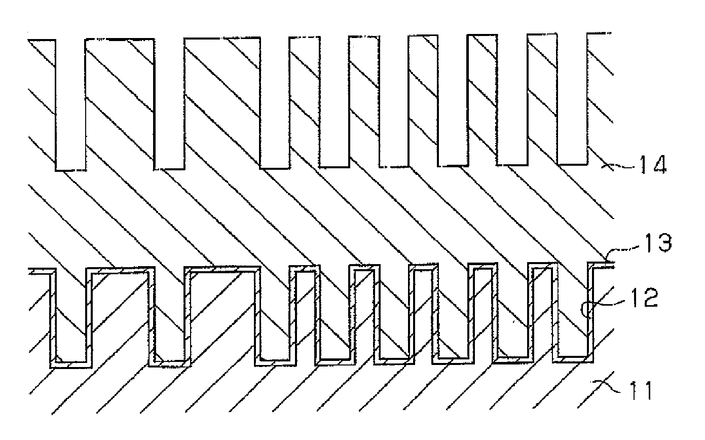
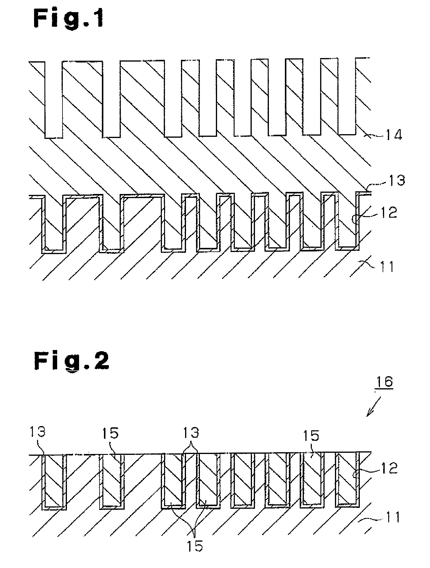
[0011]One embodiment of the present invention will now be described with reference to FIGS. 1 and 2.

[0012]First of all, a method for forming conductor wiring 15 (see FIG. 2) on a semiconductor device will be described. When the conductor wiring 15 of a semiconductor device is formed, as shown in FIG. 1, first a barrier layer 13 and a conductor layer 14 are formed on an insulator layer 11 having a trench 12. The insulator layer 11 may be any one of a SiO2 film such as a TEOS film, a BSG film, a PSG film, and a BPSG film; a SiOF film; and a SiOC film. The trench 12 is formed, for example, according to a lithography technology and a pattern etching technology, which are publicly known, such that a predetermined design pattern can be provided.

[0013]The barrier layer 13 is formed on the insulator layer 11 such that the surface of the insulator layer 11 is covered with the barrier layer 13, prior to forming the conductor layer 14. The barrier layer 13 is formed, for example, according to ...


PUM

PropertyMeasurementUnit
pHaaaaaaaaaa
particle sizeaaaaaaaaaa

Abstract

A polishing composition includes more than 0.1% by mass of colloidal silica, and water, and has a pH of 6 or less. The polishing composition has the ability to polish a titanium material at a high stock removal rate. Thus, the polishing composition is suitable for use in applications for polishing a titanium-containing object.

Description

BACKGROUND OF THE INVENTION[0001]The present invention relates to a polishing composition used, for example, in polishing for forming conductor wiring for a semiconductor device, and to a polishing method using such a polishing composition.[0002]Currently, a damascene process wherein a chemical mechanical polishing (CMP) technology is used has become the main method for forming conductor wiring for a semiconductor device. When the conductor wiring is formed, first of all, a trench is formed on an insulator layer provided on a semiconductor substrate, and then a barrier layer comprising titanium or titanium nitride is formed on the insulator layer. Subsequently, a conductor layer is formed on the barrier layer such that at least the trench is filled with the conductor layer, and then a portion of the conductor layer and a portion of the barrier layer, each of which is positioned outside the trench, are removed by chemical mechanical polishing, whereby a portion of the conductor layer...

Claims


Application Information

Patent Timeline
Patent Type & Authority Applications(United States)
IPC IPC(8): B24B1/00B24B37/00C09G1/02C09K3/14H01L21/304H01L21/321
CPCC09G1/02H01L21/3212C09K3/1463C09K3/1409A47G21/14A47G2400/025
Inventor HORIKAWA, CHIYOOHNO, KOJITAMAI, KAZUSEI
Owner FUJIMI INCORPORATED
Why Eureka
Try Eureka