Plasma display panel and method for manufacturing the same
- Summary
- Abstract
- Description
- Claims
- Application Information
AI Technical Summary
Benefits of technology
Problems solved by technology
Method used
Image

Examples
first embodiment
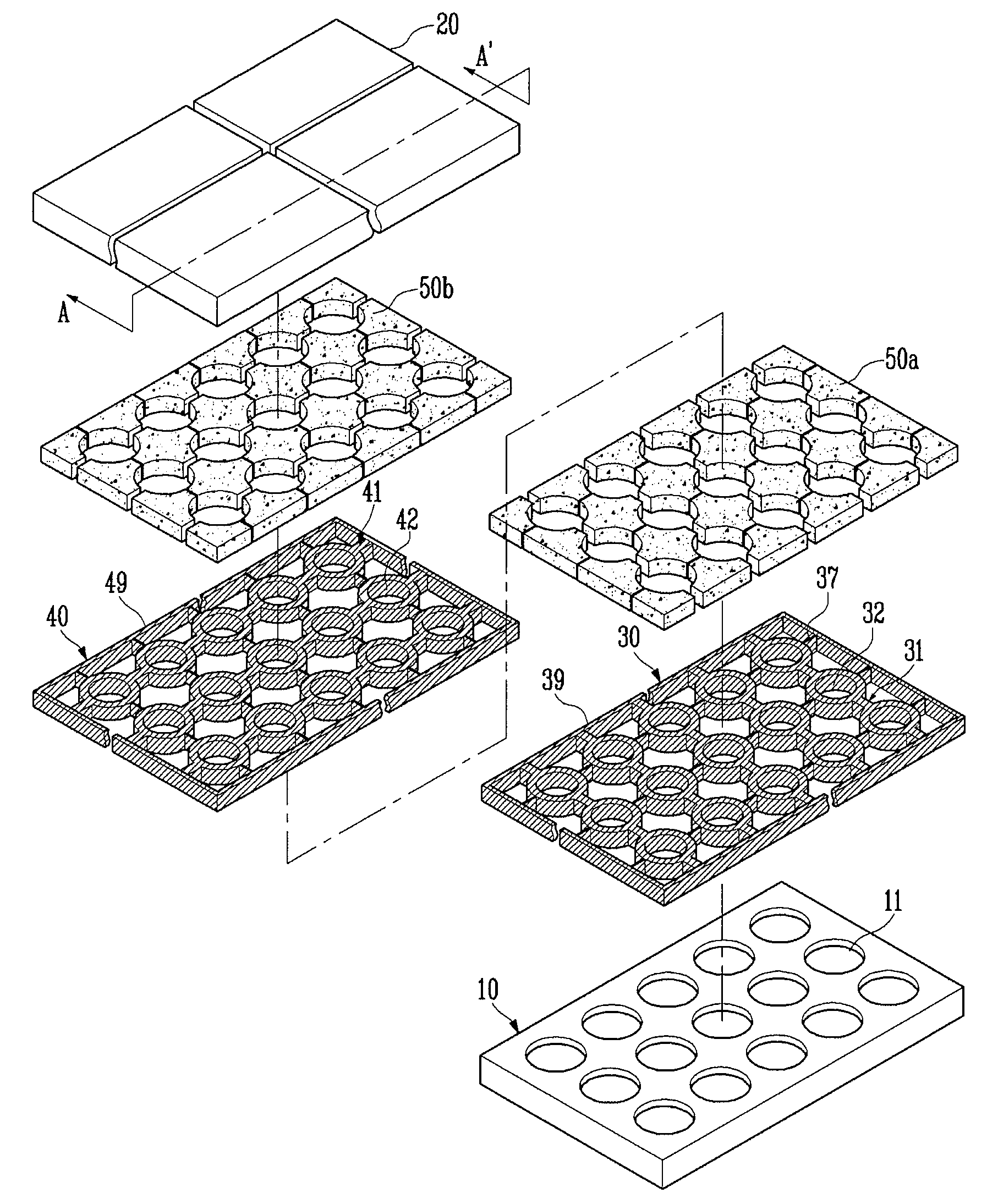
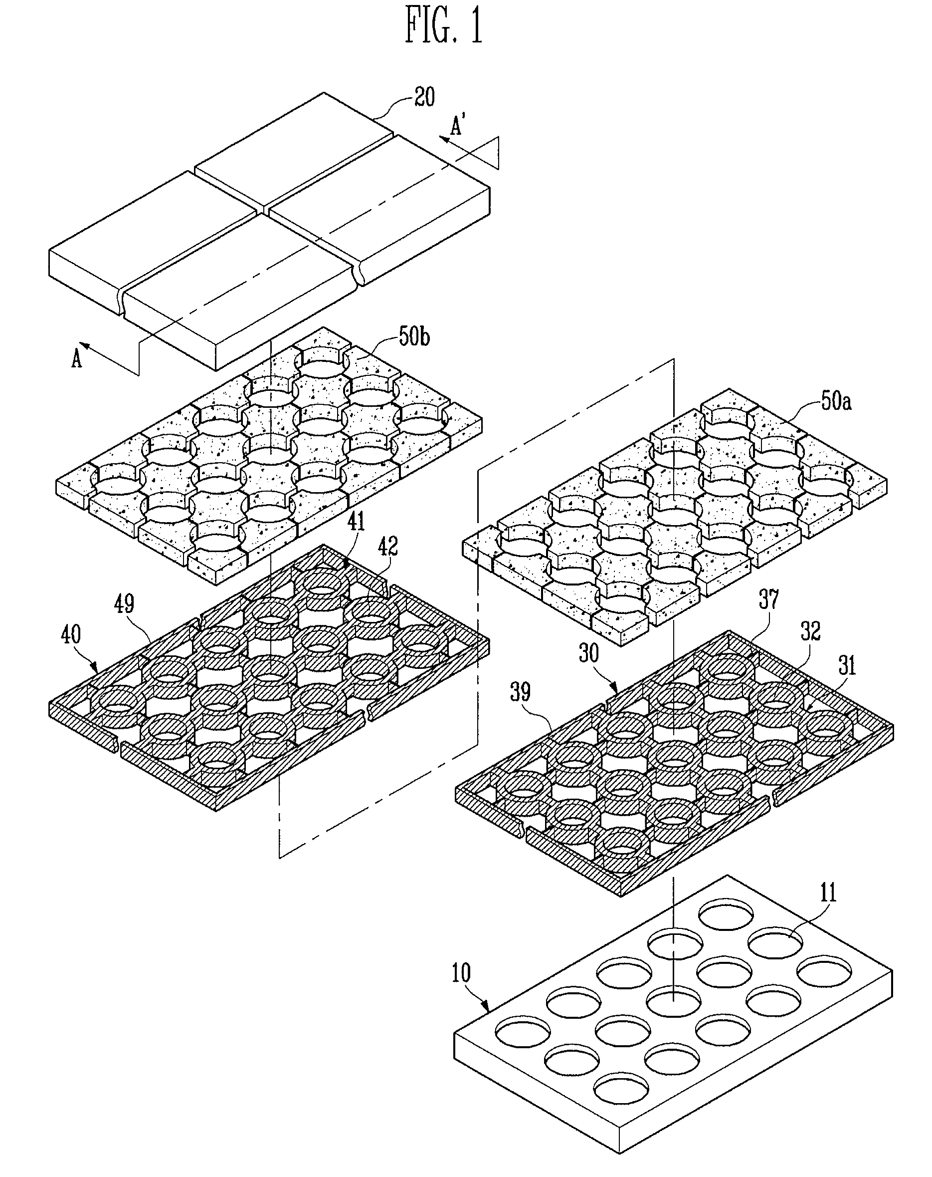
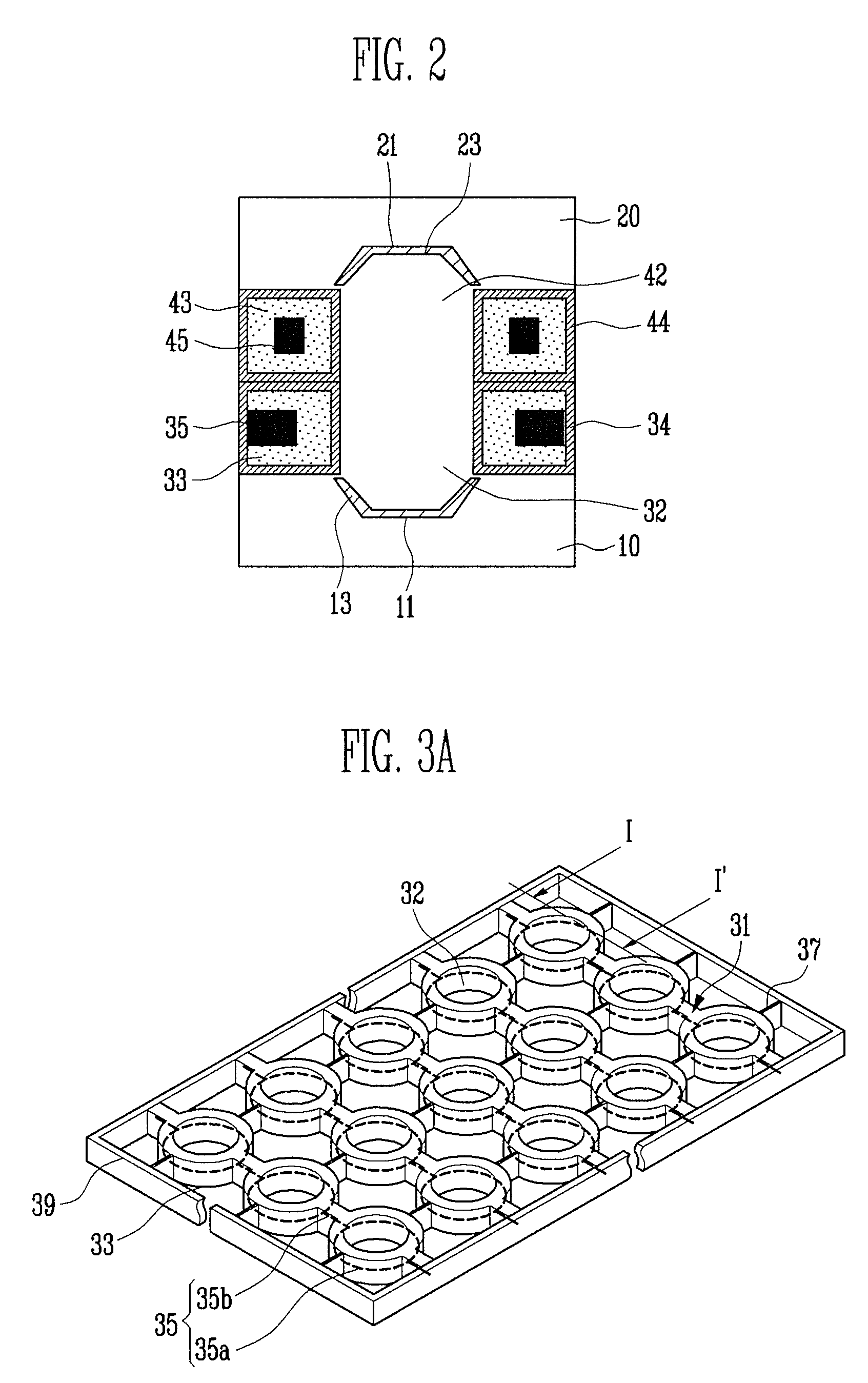
[0031]FIG. 1 is an exploded perspective view showing a plasma display panel according to the present invention. FIG. 2 is a transverse cross-sectional view of the plasma display panel shown in FIG. 1.
[0032]The plasma display panel according to the first embodiment of the present invention includes a rear substrate 10, a front substrate 20, a first electrode sheet 30, a second electrode sheet 40, and dielectric structures 50a and 50b.
[0033]The rear substrate 10 and the front substrate 20 are spaced apart from each other by a distance (that may be predetermined) therebetween. The first electrode sheet 30 and the second electrode sheet 40 are disposed between the rear substrate 10 and the front substrate 20.
[0034]As shown in FIGS. 3A and 3B, the first electrode sheet 30 includes a plurality of first inner lines 31, a first bridge line 37, and a first edge line 39. Each of the first inner lines 31 includes a first dielectric layer 33 and a first discharge electrode 35. The first bridge...
second embodiment
[0075]Each discharge space of the present invention is defined by using the rear substrate 210 as a lower surface, the front substrate 220 as an upper surface, and the discharge hole 232 formed in the electrode sheet 230 as the inner wall surface. The inside of the discharge space is filled with discharge gas.
[0076]Discharges between the first discharge electrode 211 of the rear panel 200 and the second discharge electrode 235 of the electrode sheet 230 powered by an external power source drive the plasma display panel.
[0077]For example, when the external power source is applied to the first discharge electrode 211 and the second discharge electrode 235, the first discharge electrode 211 function as a scan electrode during an address period and as Y electrode during a sustain period, and the second discharge electrode 235 function as the address electrode during the address period and an X electrode during the sustain period. Thereby driving the plasma display panel.
[0078]Since the ...
PUM
 Abstract
Description
Claims
Application Information
 - R&D Engineer
- R&D Manager
- IP Professional
- Industry Leading Data Capabilities
- Powerful AI technology
- Patent DNA Extraction
Browse by: Latest US Patents, China's latest patents, Technical Efficacy Thesaurus, Application Domain, Technology Topic.
© 2024 PatSnap. All rights reserved.Legal|Privacy policy|Modern Slavery Act Transparency Statement|Sitemap