

Transfer substrate, and fabrication process of organic electroluminescent devices
a technology of electroluminescent devices and transfer substrates, which is applied in the direction of instruments, transportation and packaging, vacuum evaporation coatings, etc., can solve the problems of reduced luminescence efficiency, reduced brightness half-life, and increased drive voltage, and achieves the effect of facilitating the formation of the transfer substrate 100′
- Summary
- Abstract
- Description
- Claims
- Application Information
AI Technical Summary
Benefits of technology
Problems solved by technology
Method used
Image

Examples
first embodiment
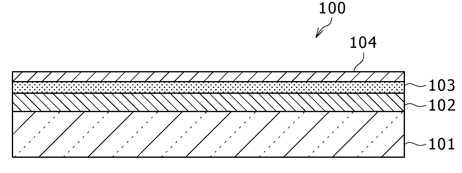
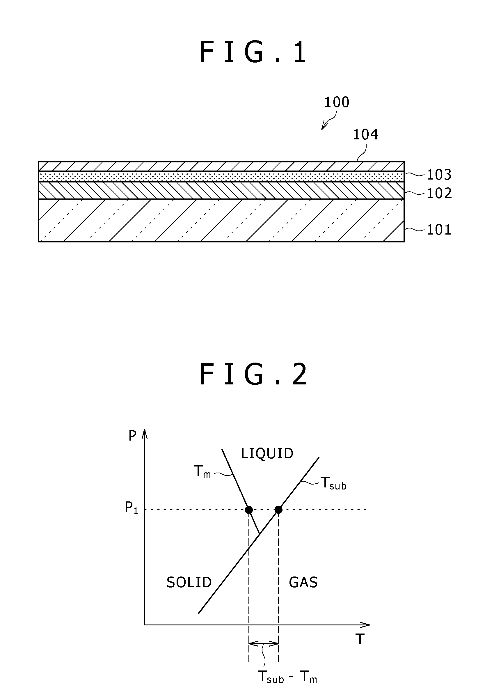
[0033]Referring first to FIG. 1, a description will hereinafter be made of the construction of a transfer substrate 100 according to the first embodiment of the present invention. The transfer substrate 100 depicted in the figure is useful, for example, for the formation of a hole transport layer in an organic electroluminescence device, and is composed of a photothermal conversion layer 102, an antioxidation layer 103 and a transfer layer 104 formed in this order on a base substrate 101.
[0034]Of these, the base substrate 101 is made of a material which transmits light hr of a predetermined wavelength to be irradiated in a transfer to be performed using the transfer substrate 100. When a laser beam of approx. 800 nm wavelength from a solid-state laser source is employed as this light hr, for example, a glass substrate may be used as the base substrate 101.
[0035]The photothermal conversion layer 102 is formed using a material, which has a high photothermal conversion efficiency in co...
second embodiment
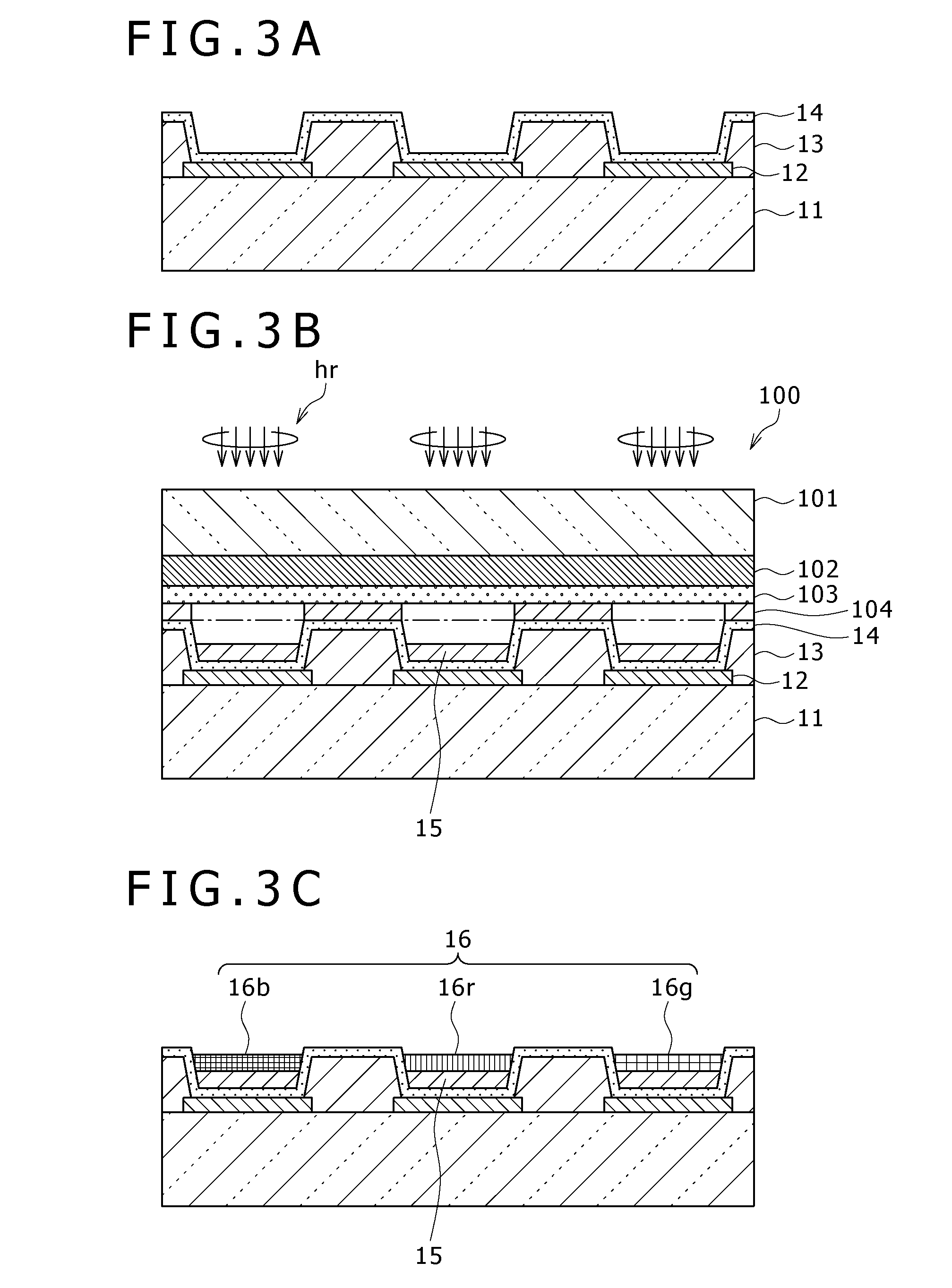
[0088]FIG. 4 is a cross-sectional construction diagram of a transfer substrate 100′ for use in this embodiment. It is to be noted that like elements of structure to those in the first embodiment will be described by applying like reference numerals. As depicted in this figure, the transfer substrate 100′ is constructed by successively stacking a photothermal conversion layer 102, an antioxidant layer 103 and a transfer layer 104′ on a base substrate 101.
[0089]In this embodiment, the transfer layer 104′ is formed by stacking at least three organic material layers one over another. Described specifically, the transfer 104′ layer is constructed by successively stacking a first layer 104a′, a second layer 104b′ and a third layer 104c′ from the side of the base substrate 101.
[0090]The first layer 104a′ on the side of the base substrate 101 and the third layer 104c′ on the side of the surface are each formed with an organic material selected from the group including a first organic materi...
examples
[0102]A description will next be made of fabrication procedures of organic electroluminescent devices of specific examples of the present invention and comparative examples to these specific examples and also of their evaluation results.
PUM
| Property | Measurement | Unit |
|---|---|---|
| Tm | aaaaa | aaaaa |
| melting point | aaaaa | aaaaa |
| organic | aaaaa | aaaaa |
Abstract
Description
Claims
Application Information