Semiconductor device and electronic device using the same

Active Publication Date: 2008-10-09
SEMICON ENERGY LAB CO LTD
View PDF47 Cites 57 Cited by
  • Summary
  • Abstract
  • Description
  • Claims
  • Application Information

AI Technical Summary

Benefits of technology

[0079]By using the present invention, a semiconductor device which can detect low illuminance can be obtained. In addition, a semiconductor device which operates at low voltage, a semicondu

Problems solved by technology

A conventional optical sensor has a problem in that illuminance which is quite low is difficult to be detected due to limitation of characteristics of a transistor even when low illuminance is to be detected. FIG. 33A shows a circuit diag

Method used


Image

  • Semiconductor device and electronic device using the same
  • Semiconductor device and electronic device using the same
  • Semiconductor device and electronic device using the same

Examples


embodiment mode 2

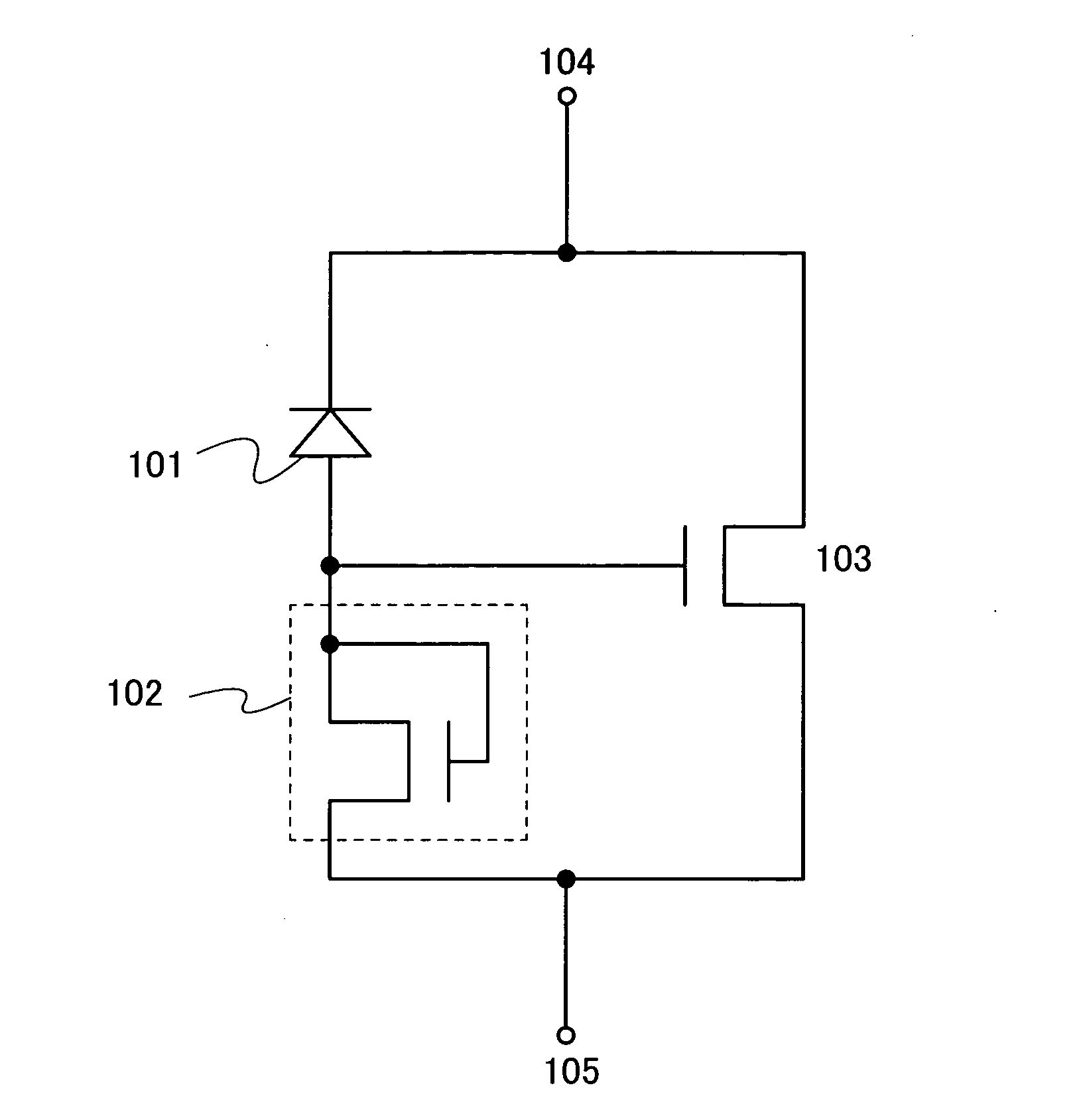
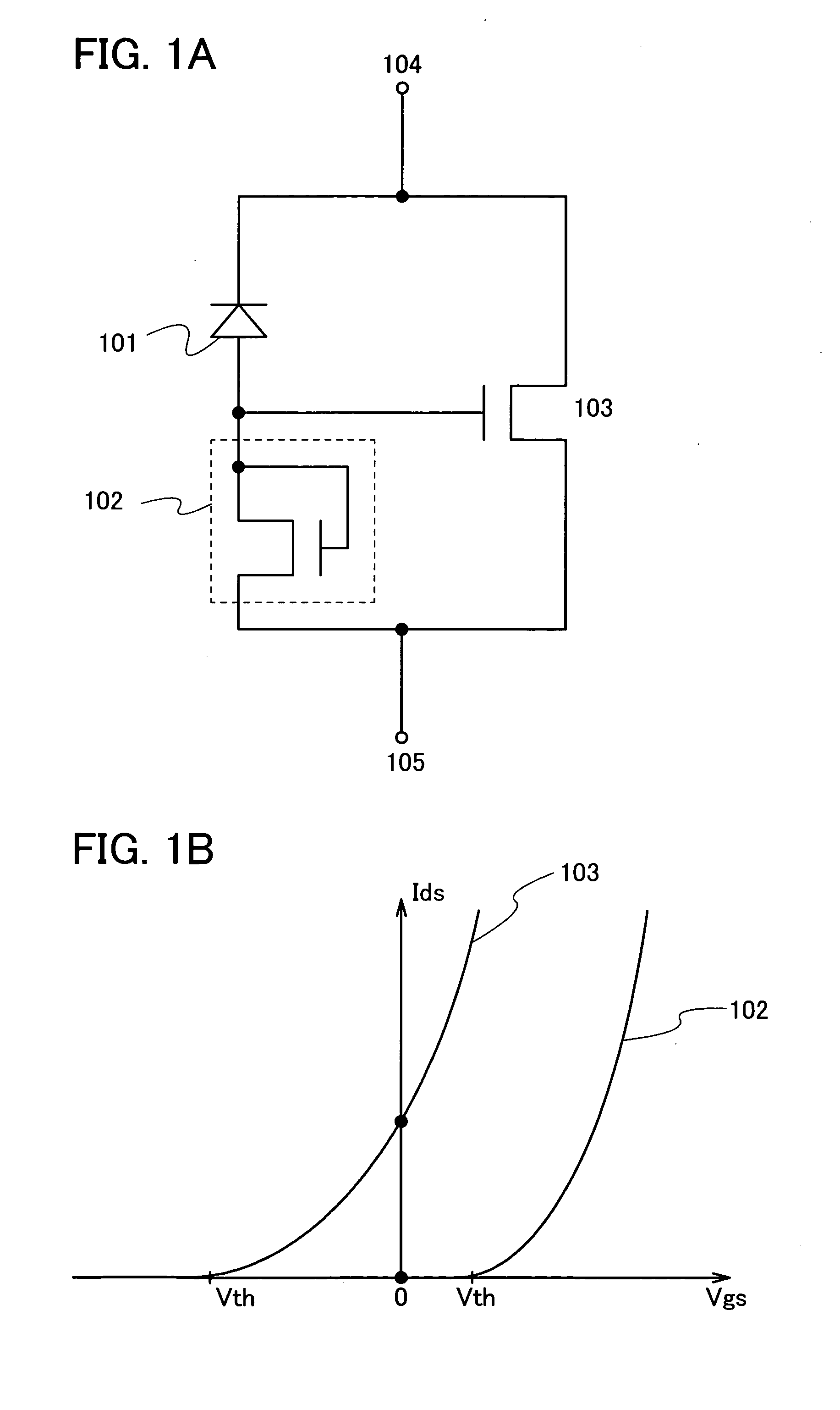
[0149]The case where the first circuit 102 is a diode-connected N-channel transistor is described in Embodiment Mode 1. Note that the present invention is not limited to this, and various structures can be used for the first circuit 102. For example, as shown in FIG. 3, a current-voltage conversion circuit 102A may be used for the first circuit 102.

[0150]Connection relationships of the case where a photodiode is used as an example of the photoelectric conversion element 101 are described below. In FIG. 3, a cathode terminal of the photodiode is connected to the first terminal 104 and an anode terminal of the photodiode is connected to a first terminal of the current-voltage conversion circuit 102A. The first terminal of the current-voltage conversion circuit 102A is connected to the gate (or the gate electrode) of the N-channel transistor included in the second circuit 103. A second terminal of the current-voltage conversion circuit 102A is connected to the second terminal 105.

[0151...

embodiment mode 3

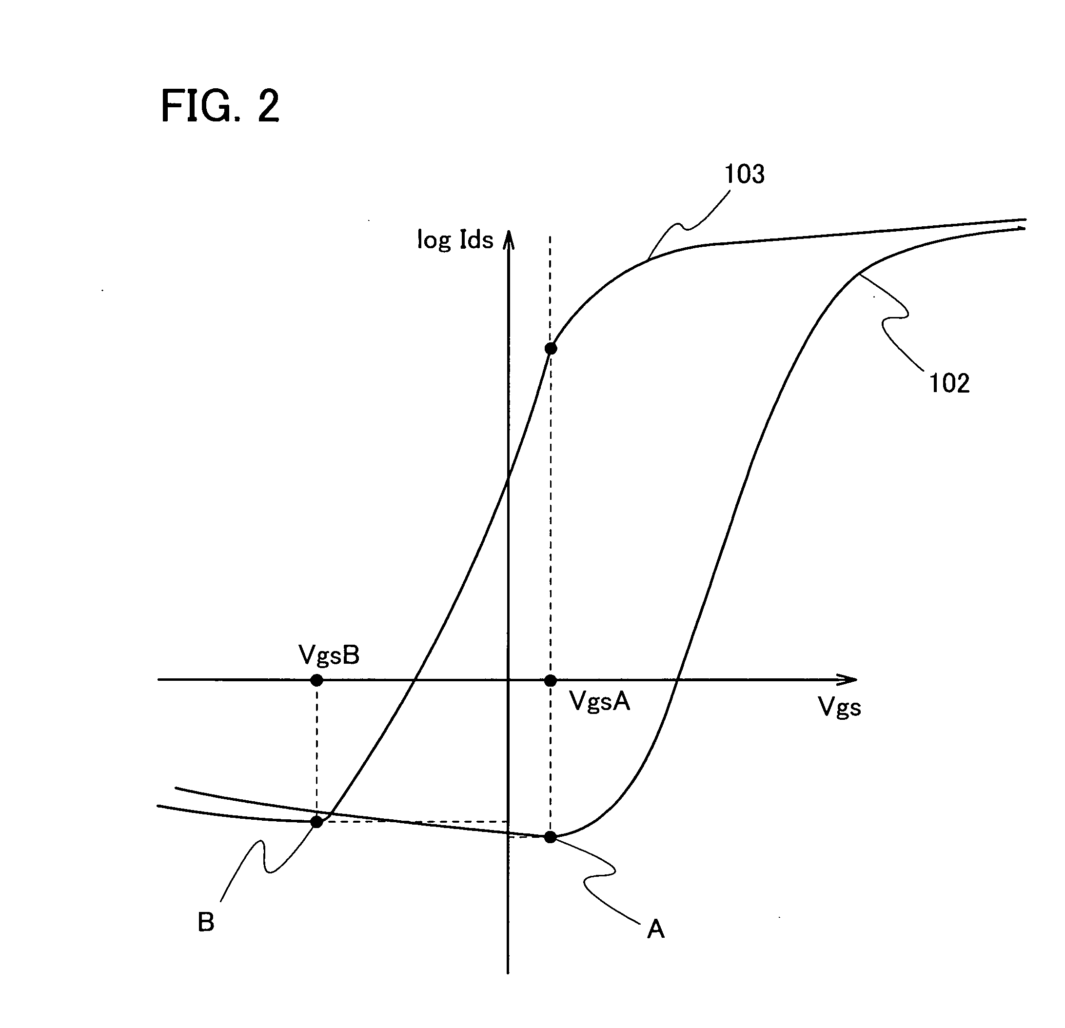
[0167]The case where output current increases as intensity of light emitted to the photoelectric conversion element 101 increases is shown in Embodiment Modes 1 and 2. In this embodiment mode, the case where output current decreases as intensity of light emitted to the photoelectric conversion element 101 increases is shown.

[0168]FIG. 8 shows a diagram of this embodiment mode which corresponds to FIG. 1A. In FIG. 8, a connection between the photoelectric conversion element 101 and an N-channel transistor included in a first circuit 802 is different from that of FIG. 1A.

[0169]A semiconductor device shown in FIG. 8 includes the photoelectric conversion element 101, a first circuit 802, a second circuit 803, the first terminal 104, and the second terminal 105. The first circuit 802 is connected to the photoelectric conversion element 101 in series. In addition, the first circuit 802 has a function of generating voltage in accordance with input current, e.g., current flowing to the phot...

embodiment mode 4

[0190]In Embodiment Mode 2, the case where various structures are used for the first circuit 102 in Embodiment Mode 1 is described. Meanwhile, in Embodiment Mode 3, the case where a connection between the first circuit 102 and the photoelectric conversion element 101 is different from that of Embodiment Mode 1 is described. Thus, the case where various structures are used for the first circuit 802 in Embodiment Mode 3 is also described in this embodiment mode.

[0191]Connection relationships of the case where a photodiode is used as an example of the photoelectric conversion element 101 are described below. In FIG. 9, a cathode terminal of the photodiode is connected to a first terminal of a current-voltage conversion circuit 802A and an anode terminal of the photodiode is connected to the second terminal 105. The first terminal of the current-voltage conversion circuit 802A is connected to the gate (or the gate electrode) of the N-channel transistor included in the second circuit 803...


PUM


Abstract

To provide a semiconductor device which can detect low illuminance. A photoelectric conversion element, a diode-connected first transistor, and a second transistor are included. A gate of the first transistor is electrically connected to a gate of the second transistor. One of a source and a drain of the first transistor is electrically connected to one of a source and a drain of the second transistor through the photoelectric conversion element. The other of the source and the drain of the first transistor is electrically connected to the other of the source and the drain of the second transistor. By using transistors which have different threshold voltages for the first transistor and the second transistor, a semiconductor device which can perform detecting of low illuminance can be obtained.

Description

BACKGROUND OF THE INVENTION[0001]1. Field of the Invention[0002]The present invention relates to a semiconductor device. In particular, the present invention relates to a semiconductor device having a photoelectric conversion device and a transistor. Further, the present invention relates to an electronic device using such a semiconductor device.[0003]2. Description of the Related Art[0004]A large number of photoelectric conversion devices generally used for detecting an electromagnetic wave are known, and for example, a photoelectric conversion device having sensitivity to ultra-violet rays to infrared rays is collectively referred to as an optical sensor. An optical sensor having sensitivity to a visible light region with a wavelength of 400 to 700 nm is particularly referred to as a visible light sensor. A large number of visible light sensors are used for devices which need illuminance adjustment, on / off control, or the like depending on human living environment.[0005]In particu...

Claims


Application Information

Patent Timeline
IPC IPC(8): H01L27/146H01L31/10
CPCH01L27/14609H01L27/14643H01L27/14692H04N5/374H04N3/155H04N5/355H01L31/1055H04N25/573H04N25/76H04N25/57
Inventor KIMURA, HAJIME
Owner SEMICON ENERGY LAB CO LTD
Why Eureka
Try Eureka