Pillar-type field effect transistor having low leakage current

a field effect transistor and low leakage current technology, applied in semiconductor devices, digital storage, instruments, etc., can solve the problems of so-called short channel effect, the thickness of the gate insulating layer cannot be greatly reduced in terms of device characteristics, and the aforementioned short channel effect problem becomes serious

Inactive Publication Date: 2008-10-16
SEOUL NAT UNIV R&DB FOUND
View PDF1 Cites 60 Cited by
  • Summary
  • Abstract
  • Description
  • Claims
  • Application Information

AI Technical Summary

Benefits of technology

[0010]The present discussion provides, inter alia, a pillar-type field effect transistor having a reduced cell device area, having good miniaturization characteristics, and minimizing an off-state leakage current, to be used as a highly-integrated DRAM cell.
[0012]The present discussion also provides a pillar-type FET capable of obtaining an excellent degree of device integration and reducing an off-state leakage current by adjusting a cross-sectional area of a semiconductor pillar and a thickness of a gate insulating layer.

Problems solved by technology

As a problem in the miniaturization of cell devices, there is a so-called short channel effect problem.
If the conventional MOSFET having the planar channel region is adapted to a sub-100 nm DRAM technology, the aforementioned short channel effect problem becomes serious.
In comparison with a Logic MOSFET, in the MOSFET for a DRAM cell device, the thickness of the gate insulating layer cannot be greatly reduced in terms of device characteristics, and the depth of the source / drain regions cannot be greatly deepened.
Therefore, the miniaturization of the DRAM cell device is difficult.
Therefore, in the conventional MOSFET having the planar channel, it is very difficult to reduce the gate length of the cell device down to about 70 nm or less.
In addition, since a channel formed in the vicinity of a bottom of a buried region is formed in a concave shape, a problem of a back-bias effect become serious.
In addition, any change in doping concentration of the channel region in the vicinity of the bottom causes a great change in a threshold voltage.
In addition, in the ministration of device, a width of the buried channel region is reduced, so that it is difficult to control an etching profile in the vicinity of the bottom of the buried channel region and to maintain a uniform depth of the buried channel region.
However, the double / triple-gate MOSFET formed on a SOI substrate, that is, an SOI FinFET cannot be substantially adapted to a DRAM cell device due to its device characteristics.
In this case, since the threshold voltage of a device is decreased, there is a problem in that the off-state current is increased.
However, the increase in the doping concentration causes an increase in the leakage current due to the band-to-band tunneling between the drain region and the channel region.
There is a limitation in increasing the doping concentration for the channel region.
However, there is a problem in that peripheral circuits become complicated.
As a result, there is a problem in that the off-state current is increased.

Method used


Image

  • Pillar-type field effect transistor having low leakage current
  • Pillar-type field effect transistor having low leakage current
  • Pillar-type field effect transistor having low leakage current

Examples


first embodiment

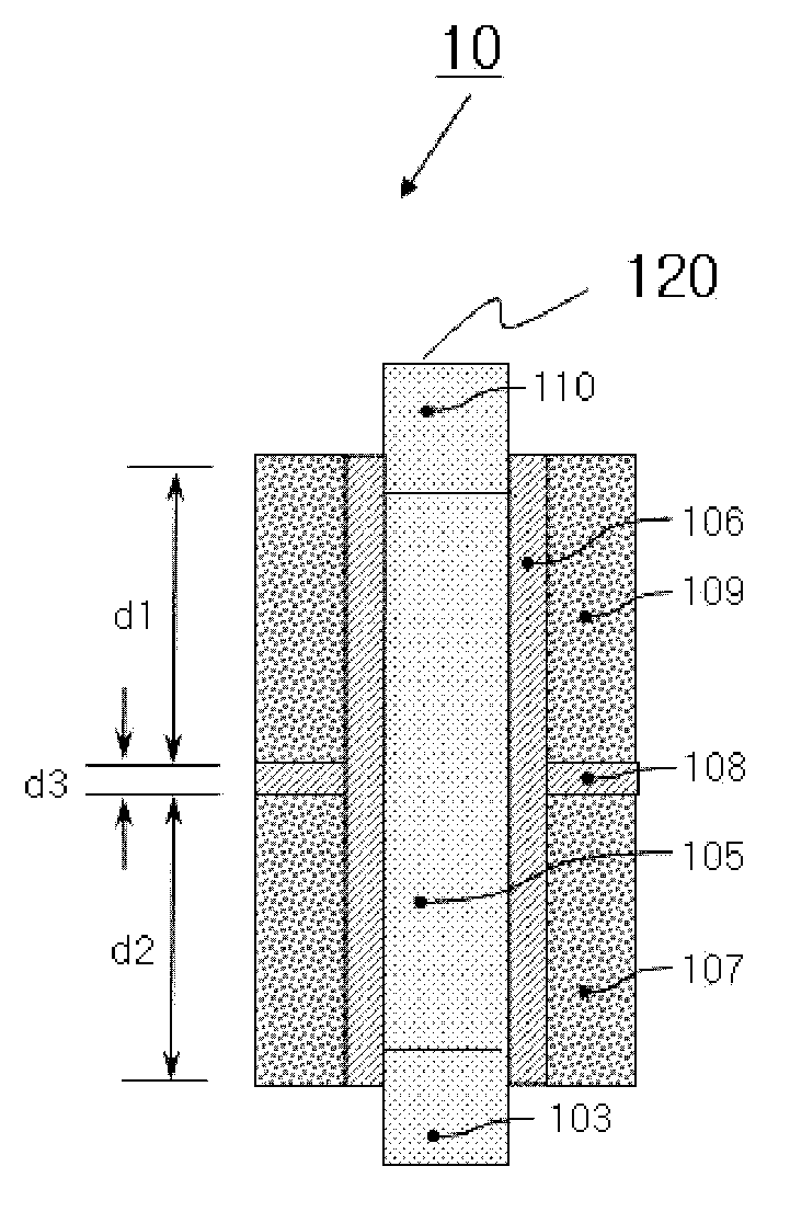
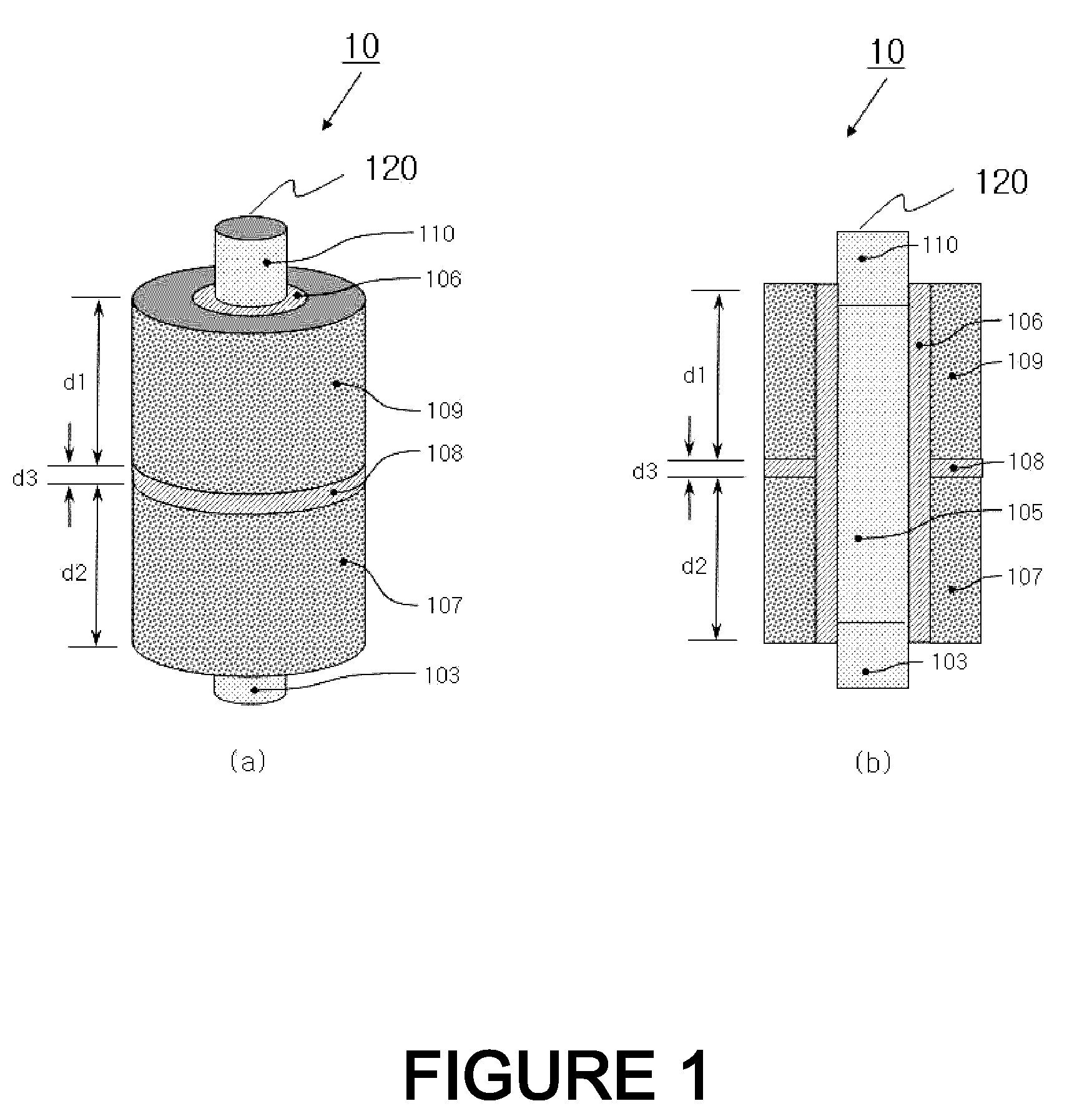
[0035]The pillar-type FET 10 includes a source 103, a body 105, a drain 110, a gate insulating layer 106, and a gate electrode. The gate electrode includes a first gate electrode 109, a second gate electrode 107, and an inter-gate insulating layer 108. The source 103, the body 105, and the drain 110 are formed in a semiconductor pillar 120 made of silicon. The semiconductor pillar may be formed on a semiconductor substrate such as a bulk silicon substrate and a silicon on insulator (SOI) substrate. The semiconductor pillar may be formed in various shapes such as circle, ellipse, corner-rounded rectangle, and corner-rounded triangle. The height of the semiconductor pillar is defined to be in a range of 50 nm to 1000 nm. The cross-sectional area of the semiconductor pillar in the horizontal direction may be formed to be uniform. Alternatively, the cross-sectional area of the semiconductor pillar may be increased or decreased in various functional forms in the upward direction. Altern...

third embodiment

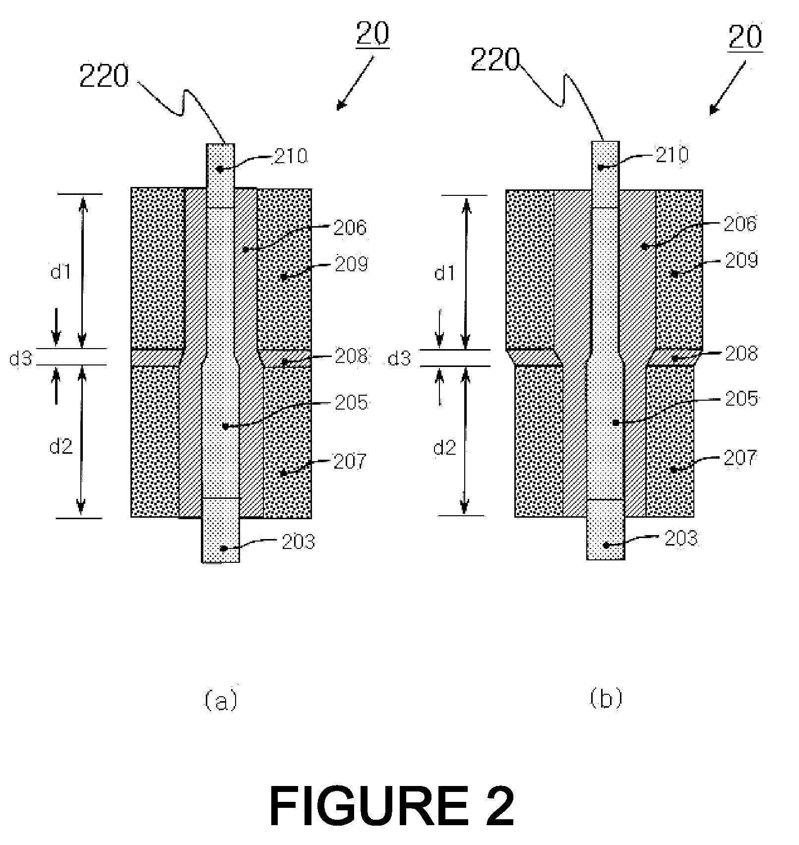
[0052]In the pillar-type FET 30 when the first gate electrode 309 and the second gate electrode 307 are formed, the first gate electrode 309 is firstly formed, and the second gate electrode 307 having different work function is formed thereon. Alternatively, the first gate electrode 309 and the second gate electrode may be formed by forming p+ polysilicon and counter-doping the resulting product with impurities n+. A total length of the gate electrode is a sum of a length d1 of the first gate electrode 309 and a length d2 of the second gate electrode 307.

[0053]Hereinafter, structures of pillar-type FETs having low leakage current according to fourth and fifth embodiments of the present discussion will be described with reference to FIGS. 4 (a) and (b). FIG. 4 (a) is a perspective view illustrating the pillar-type FET according to the fourth embodiment of the present discussion. FIG. 4 (b) is a perspective view illustrating the pillar-type FET according to the fifth embodiment of th...


PUM


Abstract

A pillar-type field effect transistor having low leakage current is provided. The pillar-type field effect transistor includes a semiconductor pillar, a gate insulating layer formed on a portion of a surface of the semiconductor pillar, a gate electrode formed on the gate insulating layer, and source / drain regions formed on portions of the semiconductor pillar where the gate electrode is not formed, in which the gate electrode includes a first gate electrode, a second gate electrode, and an inter-gate insulating layer, in which the first gate electrode has a work function higher than that of the second gate electrode, in which the inter-gate insulating layer is formed between the first gate electrode and the second gate electrode, and in which the first gate electrode and the second gate electrode are electrically connected by a contact or a metal interconnection line. A portion of the second gate electrode having the work function lower than that of the first gate electrode is overlapped by the drain region. Accordingly, the gate electrode of the pillar-type FET is formed using a material having a high work function, so that the threshold voltage can be increased and the work function of the portion of the gate electrode overlapped by the drain region can be decreased. Therefore, gate induced drain leakage is reduced, so that off-state leakage current can likewise be greatly reduced.

Description

CROSS-REFERENCE TO RELATED APPLICATION[0001]This application claims the benefit of Korean Patent Application No. 10-2007-0035277, filed on Apr. 10, 2007, in the Korean Intellectual Property Office, the disclosure of which is incorporated herein in its entirety by reference.INTRODUCTION[0002]The present discussion relates to a pillar-type field effect transistor having low leakage current, and more particularly, to a pillar-type field effect transistor capable of reducing gate induced drain leakage by forming a semiconductor pillar on a semiconductor substrate and forming gate electrodes having different work functions so as to lower the work function of a gate electrode in a region overlapped by a drain region.BACKGROUND[0003]DRAM technology has been one of the important technologies in silicon semiconductor markets. Recently, the DRAM technology has been more actively researched to implement next-generation highly-integrated DRAMs. In particular, a gate length of a DRAM cell device...

Claims


Application Information

Patent Timeline
Patent Type & Authority Applications(United States)
IPC IPC(8): H01L29/78H01L27/108
CPCG11C11/403H01L27/10876H01L29/42392H01L29/7827H01L29/7831H01L29/78642H01L29/78648H10B12/053H01L29/4983H10B12/0383
Inventor LEE, JONG-HO
Owner SEOUL NAT UNIV R&DB FOUND
Why Eureka
Try Eureka