Pillar-type field effect transistor having low leakage current

a field effect transistor and low leakage current technology, applied in semiconductor devices, digital storage, instruments, etc., can solve the problems of serious short channel effect problem, inability to greatly reduce the thickness of the gate insulating layer in terms of device characteristics, and the so-called short channel effect, etc., to achieve excellent device integration, reduce off-state leakage current, and low leakage current

Active Publication Date: 2011-05-26
SEOUL NAT UNIV R&DB FOUND
View PDF5 Cites 26 Cited by
  • Summary
  • Abstract
  • Description
  • Claims
  • Application Information

AI Technical Summary

Benefits of technology

[0012]The present invention provides to a pillar-type field effect transistor having a reduced area of cell device, having a good miniaturization characteristic, and minimizing an off-state leakage current to be used as a highly-integrated DRAM cell.
[0014]The present invention also provides to a pillar-type FET capable of obtaining an excellent degree of device integration and reducing an off-state leakage current by adjusting a cross-sectional area of a semiconductor body and a thickness of a gate insulating layer.

Problems solved by technology

As a problem in the miniaturization of cell devices, there is a so-called short channel effect problem.
If the conventional MOSFET having the planar channel region is adapted to a sub-100 nm DRAM technology, the aforementioned short channel effect problem becomes serious.
In comparison with a Logic MOSFET, in the MOSFET for a DRAM cell device, the thickness of the gate insulating layer cannot be greatly reduced in terms of device characteristics, and the depth of the source / drain regions cannot be greatly deepened.
Therefore, the miniaturization of the DRAM cell device is difficult.
Therefore, in the conventional MOSFET having the planar channel, it is very difficult to reduce the gate length of the cell device down to about 70 nm or less.
In addition, since a channel formed in the vicinity of a bottom of a buried region is formed in a concave shape, a problem of a back-bias effect become serious.
In addition, any change in doping concentration of the channel region in the vicinity of the bottom causes a great change in a threshold voltage.
In addition, in the ministration of device, a width of the buried channel region is reduced, so that it is difficult to control an etching profile in the vicinity of the bottom of the buried channel region and to maintain a uniform depth of the buried channel region.
However, the double / triple-gate MOSFET formed on a SOI substrate, that is, an SOI FinFET cannot be substantially adapted to a DRAM cell device due to its device characteristics.
In this case, since the threshold voltage of a device is decreased, there is a problem in that the off-state current is increased.
However, the increase in the doping concentration causes an increase in the leakage current due to the band-to-band tunneling between the drain region and the channel region.
There is a limitation in increasing the doping concentration for the channel region.
However, there is a problem in that peripheral circuits become complicated.
As a result, there is a problem in that the off-state current is increased.

Method used


Image

  • Pillar-type field effect transistor having low leakage current
  • Pillar-type field effect transistor having low leakage current
  • Pillar-type field effect transistor having low leakage current

Examples


first embodiment

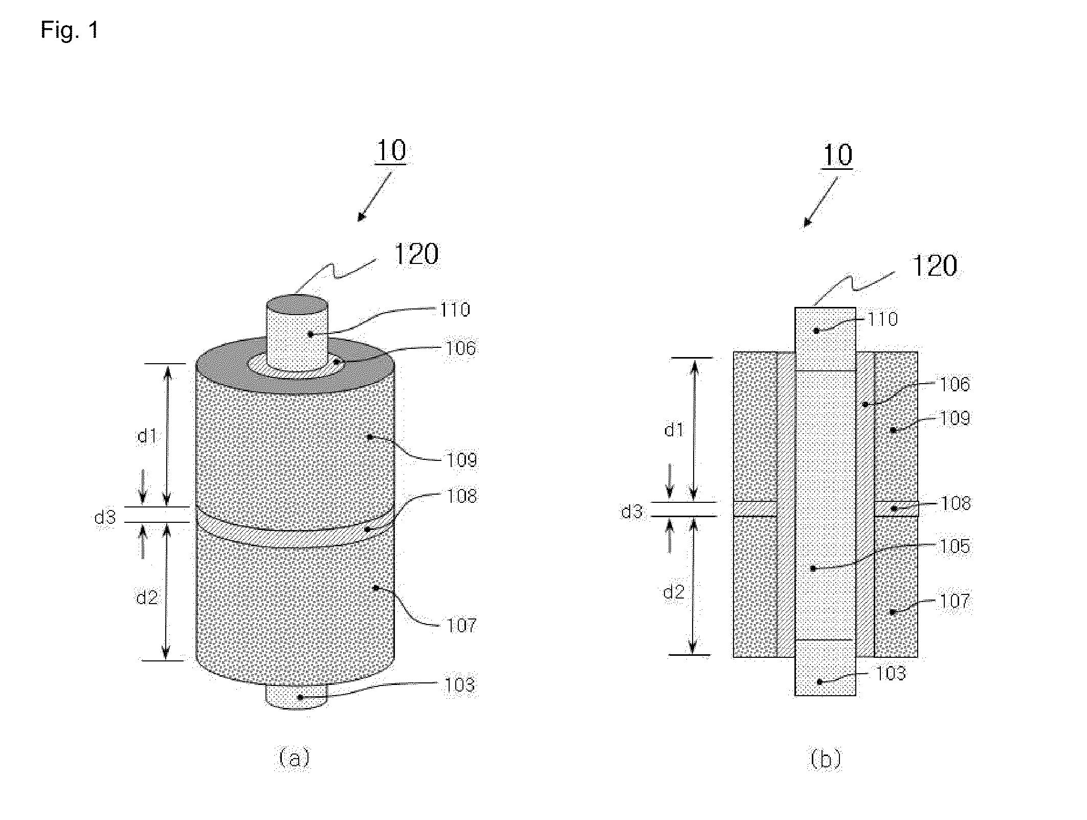
[0031]Hereinafter, a structure of a pillar-type FET having low leakage current according to a first embodiment of the present invention will be described with reference to FIG. 1. FIG. 1 illustrates the pillar-type FET having low leakage current according to the first embodiment of the present invention; and (a) and (b) are a perspective view and a cross-sectional view illustrating the pillar-type FET according to the first embodiment of the present invention, respectively. For the convenience of description, FIG. 1 illustrates only the main components excluding a semiconductor substrate, metal layers for interconnection of devices, contacts, and some insulating layers.

[0032]The pillar-type FET 10 according to the first embodiment of the present invention includes a source 103, a semiconductor body 105, a drain 110, a gate insulating layer 106, and a gate electrode. The gate electrode includes a first gate electrode 109, a second gate electrode 107, and an inter-gate insulating laye...

second embodiment

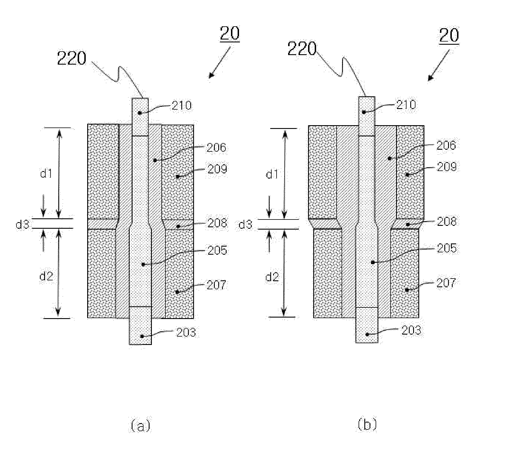
[0045]Hereinafter, a structure of a pillar-type FET having low leakage current according to a second embodiment of the present invention will be described with reference to FIG. 2. FIG. 2 illustrates the pillar-type FET having low leakage current according to the second embodiment of the present invention; and (a) and (b) are cross-sectional views illustrating first and second examples of the pillar-type FET according to the second embodiment, respectively. For the convenience of description, FIG. 2 illustrates only the main components excluding a semiconductor substrate, metal layers for interconnection of devices, contacts, and some insulating layers.

[0046]The pillar-type FET according to the second embodiment is the same as the pillar-type FET according to the first embodiment except for a thickness of a gate insulating layer and a width of a semiconductor pillar. Referring to FIG. 2 (a), in the pillar-type FET according to the second embodiment, a width of the semiconductor pill...

third embodiment

[0049]Hereinafter, a structure of a pillar-type FET having low leakage current according to a third embodiment of the present invention will be described with reference to FIG. 3. FIG. 3 is a perspective view illustrating the pillar-type FET according to the third embodiment of the present invention. For the convenience of description, FIG. 3 illustrates only the main components excluding a semiconductor substrate, metal layers for interconnection of devices, contacts, and some insulating layers.

[0050]Referring to FIG. 3, the pillar-type FET 30 according to the third embodiment is implemented by modifying only the gate electrode of the pillar-type FET according to the first embodiment. More specifically, the pillar-type FET according to the third embodiment is implemented by removing an inter-gate insulating layer between the first gate electrode 307 and the second gate electrode 309. Structures and characteristics of other components of the pillar-type FET 30 according to the third...


PUM


Abstract

A pillar-type field effect transistor having low leakage current is provided. The pillar-type field effect transistor includes: a semiconductor body, source and drain formed in a semiconductor pillar; a gate insulating layer formed on a surface of the semiconductor body; a gate electrode formed on a surface of the gate insulating layer. The gate electrode includes a first gate electrode and a second gate electrode being electrically connected with the first gate electrode. The first gate electrode has a work function higher than that of the second gate electrode. Accordingly, the gate induced drain leakage (GIDL) can be reduced, so that an off-state leakage current can be greatly reduced.

Description

CROSS-REFERENCE TO RELATED PATENT APPLICATION[0001]This application is a continuation-in-part of U.S. patent application Ser. No. 12 / 101,143, filed on Apr. 10, 2008, in the name of Jong-Ho LEE. This application claims the benefit of Korean Patent Application No. 10-2007-0035277, filed on Apr. 10, 2007, in the Korean Intellectual Property Office, the disclosure of which is incorporated herein in its entirety by reference.BACKGROUND OF THE INVENTION[0002]1. Field of the Invention[0003]The present invention relates to a pillar-type field effect transistor having low leakage current, and more particularly, to a pillar-type field effect transistor capable of reducing gate induced drain leakage by forming a semiconductor body on a semiconductor substrate and forming a plurality of gate electrodes having different work functions so as to lower a work function of a gate electrode in a region overlapped with a drain region.[0004]2. Description of the Related Art[0005]DRAM technology has been...

Claims


Application Information

Patent Timeline
Patent Type & Authority Applications(United States)
IPC IPC(8): H01L29/78
CPCG11C11/403H01L27/10876H01L29/42392H01L29/78648H01L29/7831H01L29/78642H01L29/7827H10B12/053
Inventor LEE, JONG-HO
Owner SEOUL NAT UNIV R&DB FOUND
Why Eureka
Try Eureka