High performance one-transistor dram cell device and manufacturing method thereof

a dram cell, one-transistor technology, applied in semiconductor devices, digital storage, instruments, etc., can solve the problems of short channel effect, difficult to sense and store information for a long time, and difficult manufacturing process for miniaturizing the cell device and the cell capacitor in the mos device, so as to reduce the dispersion of threshold voltages, improve the degree of integration of the cell array, and good miniaturization characteristics of the cell devi

Active Publication Date: 2010-04-29
SEOUL NAT UNIV R&DB FOUND
View PDF6 Cites 21 Cited by
  • Summary
  • Abstract
  • Description
  • Claims
  • Application Information

AI Technical Summary

Benefits of technology

[0026]In the aforementioned cell device according to the present invention, the upper gate electrode in the double-gate structure is constructed with a gate which is generally used for an MOS device, and the lower control electrode is constructed so as to have a non-volatile memory function. Therefore, it is possible to obtain a good miniaturization characteristic of the cell device. In addition, it is possible to reduce a dispersion of the threshold voltages by adjusting an amount of charges in the charge storage node. In addition, it is possible to improve a degree of integration of the cell array by commonly using a suitable control electrode. In addition, it is possible to improve performances of the DRAM cell device by adding a memory function to write / erase / read operations.

Problems solved by technology

Such a miniaturization of the cell device and the cell capacitor in the MOS device requires very difficult manufacturing processes.
However, due to the miniaturization of channel length, a short channel effect occurs.
Accordingly, it is difficult to sense and to store information for a long time.
However, the one-transistor DRAM cell device has the problems as follows.
Although a completely-depleted device is actually manufactured, a dispersion of the threshold voltages among the cell devices is too large, so that it is difficult to implement a practical device.
In addition, the lower gate electrode 25 needs to be independently provided to each cell device, there is a problem in that a degree of integration of cell devices is greatly decreased in a layout of a cell array of the cell devices.
Although the sensing margin can be improved due to the double-gate effect, the one-transistor DRAM cell device has the problems as follows.
However, if the thickness is reduced, much difficulty is involved with the processes.
Secondly, since the substrate 1 is used as the lower gate electrode, the substrate is common to the all cell devices, so that it is impossible to apply a bias to a specific cell device or to cell device in a specific region.
However, in this case, since an interval between the wells needs to be enlarged, a degree of integration is greatly decreased.
Thirdly, as described in FIG. 2 (a), since a completely-depleted floating body needs to be used, there is an elementary problem in that a dispersion of read currents among the cell devices is increased.
However, according to the published result, a change in threshold voltage in the write / erase operations in the device is not good.
However, there is no published one-transistor DRAM cell device using the structure.
If the structure is directly adapted to the one-transistor DRAM cell device, there are problems as follows.
Secondly, since the bottom electrodes 23 formed in the substrate 1 are not electrically isolated between the cell devices, a lower electrode effect for a specific cell device or for a plurality of cell devices in a specific region cannot be reduced.
In this case, since an interval between the bottom electrodes 23 of the cell devices needs to be enlarged so as to electrically independently provide the bottom electrodes 23 to the cell devices, there is a problem in that a degree of integration in a cell array of the cell device is greatly decreased.
Thirdly, as described above with reference to FIGS. 2 (a) and (b), since the dispersion of the threshold voltages among the cell devices having completely-depleted floating body 3 is too large, it is difficult to practically implement the one-transistor DRAM cell device without a special method.

Method used


Image

  • High performance one-transistor dram cell device and manufacturing method thereof
  • High performance one-transistor dram cell device and manufacturing method thereof
  • High performance one-transistor dram cell device and manufacturing method thereof

Examples


Embodiment Construction

[0039]Hereinafter, exemplary embodiments of the present invention will be described with reference to the accompanying drawings. The embodiments are provided to the skilled person in the related art for the better understanding of principles of the present invention. Therefore, the present invention is not limited to the embodiments, but various modifications can be implemented. In the description of the present invention, an NMOS device cell is assumed if there is no specific mention. All the description and principles can be adapted to a PMOS cell.

[0040]One-Transistor DRAM Cell Device

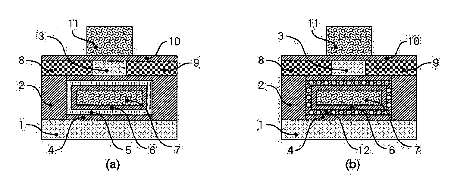
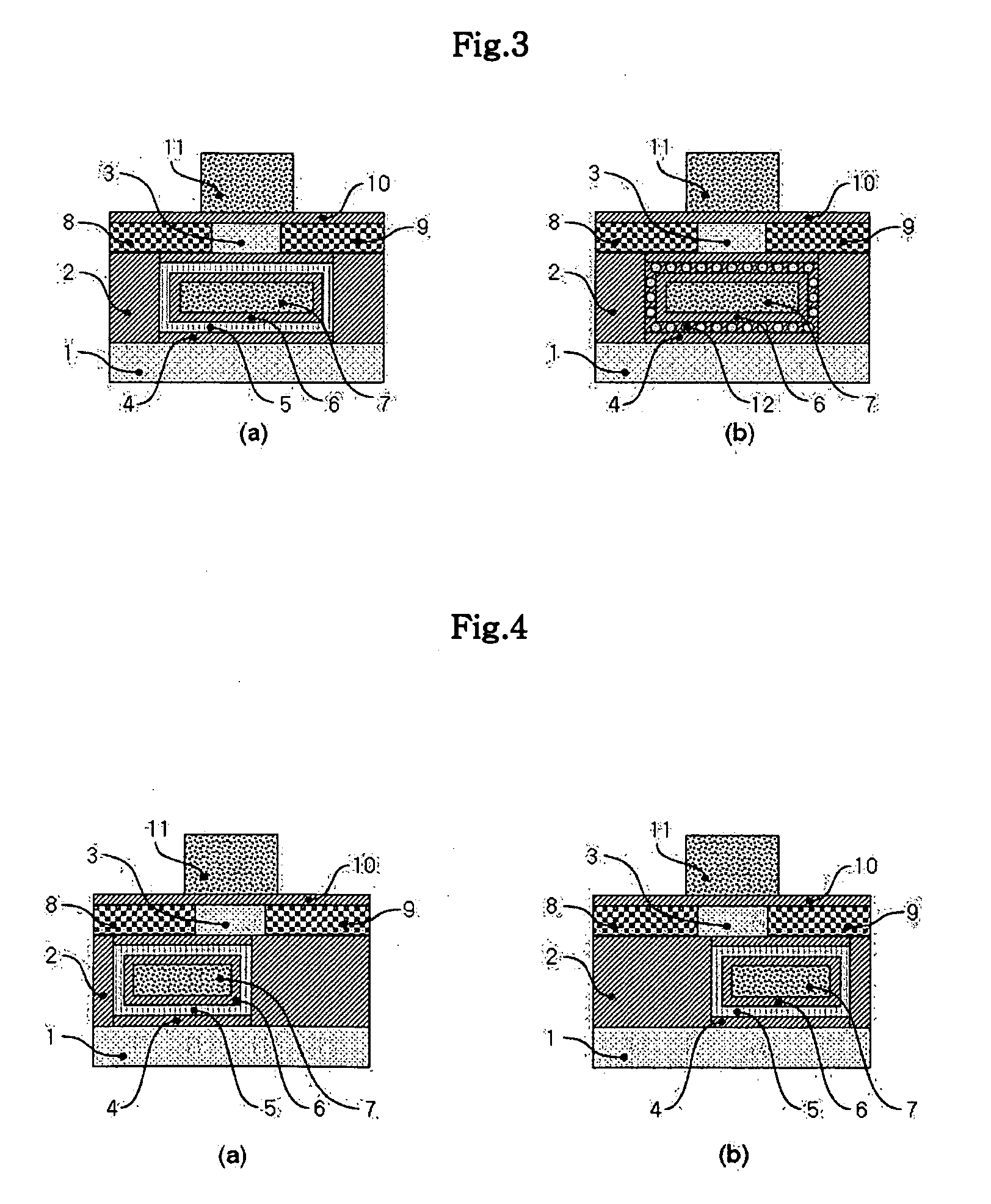
[0041]A structure of a one-transistor DRAM cell device according to a first embodiment of the present invention will be described with reference to FIG. 3. FIG. 3 (a) is a cross-sectional view showing the structure of the one-transistor DRAM cell device according to the first embodiment. In the structure, a source 8, a drain 9, and a floating body 3 are formed in a silicon film, and a gate electrode 1...


PUM


Abstract

Provided are a high-performance one-transistor floating-body DRAM cell device and a manufacturing method thereof. The one-transistor floating-body DRAM cell device includes: a semiconductor substrate; a gate stack which is formed on the semiconductor substrate; a control electrode which is formed on the semiconductor substrate and surrounded by the gate stack; a floating body which is formed on the control electrode that is surrounded by the gate stack; source/drain which are formed at left and right sides of the floating body; an insulating layer which insulates the source/drain from the semiconductor substrate and the control electrode; a gate insulating layer which is formed on the floating body and the source/drain; and a gate electrode which is formed on the gate insulating layer. In the cell device having a double-gate structure, charges can be stored in a non-volatile manner by the control electrodes, so that it is possible to improve a degree of integration of devices, a uniformity of characteristic, and a sensing margin.

Description

CROSS-REFERENCE TO RELATED PATENT APPLICATION[0001]This application claims the benefit of Korean Patent Application No. 10-2007-0086516, filed on Aug. 28, 2007, in the Korean Intellectual Property Office, the disclosure of which is incorporated herein in its entirety by reference.BACKGROUND OF THE INVENTION[0002]1. Field of the Invention[0003]The present invention relates to a device structure of a semiconductor device, particularly, a MOS transistor and a manufacturing method thereof, and more particularly, a high-performance one-transistor floating-body DRAM cell device having a double-gate structure where the one gate is a gate of a general MOS device and the other is a control electrode having a non-volatile memory function, a manufacturing method thereof, and a cell array of the devices.[0004]2. Description of the Related Art[0005]An existing DRAM cell device is constructed with one MOS transistor and one cell capacitor. Recently, as a degree of integration in a DRAM is increas...

Claims


Application Information

Patent Timeline
Patent Type & Authority Applications(United States)
IPC IPC(8): H01L27/108H01L21/84
CPCG11C11/404G11C2211/4016H01L29/7841H01L27/10802H01L27/108H10B12/20H10B12/00
Inventor LEE, JONG-HOPARK, KI-HEUNG
Owner SEOUL NAT UNIV R&DB FOUND
Why Eureka
Try Eureka