Magnetoresistance effect element and magnetoresistive random access memory using the same

a random access memory and magnetoresistance effect technology, applied in the manufacture of flux-sensitive heads, solid-state devices, instruments, etc., can solve the problems of inability to allow a device to operate as a memory, inability to achieve a small cell size, and decrease in the thermal stability required for the data retention characteristics of a non-volatile memory

Active Publication Date: 2008-10-16
KIOXIA CORP
View PDF5 Cites 85 Cited by
  • Summary
  • Abstract
  • Description
  • Claims
  • Application Information

AI Technical Summary

Problems solved by technology

This makes it difficult to achieve a small cell size for obtaining a large capacity exceeding 256 Mbits and a low writing electric current at the same time.
Unfortunately, the following problem arises when implementing an MRAM by using the spin transfer torque writing method.
This practically makes it impossible to allow a device to operate as a memory by using the spin transfer torque writing method.
When the saturation magnetization is decreased by using the present techniques, however, the thermal stability required for the data retention characteristics of a non-volatile memory also decreases.

Method used


Image

  • Magnetoresistance effect element and magnetoresistive random access memory using the same
  • Magnetoresistance effect element and magnetoresistive random access memory using the same
  • Magnetoresistance effect element and magnetoresistive random access memory using the same

Examples


first embodiment

[0030]The first embodiment is directed to an MR element.

(1) Structure of MR Element

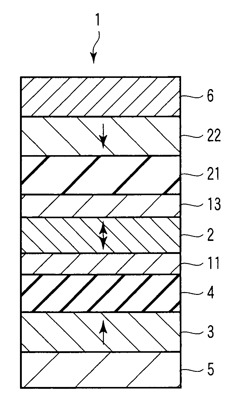
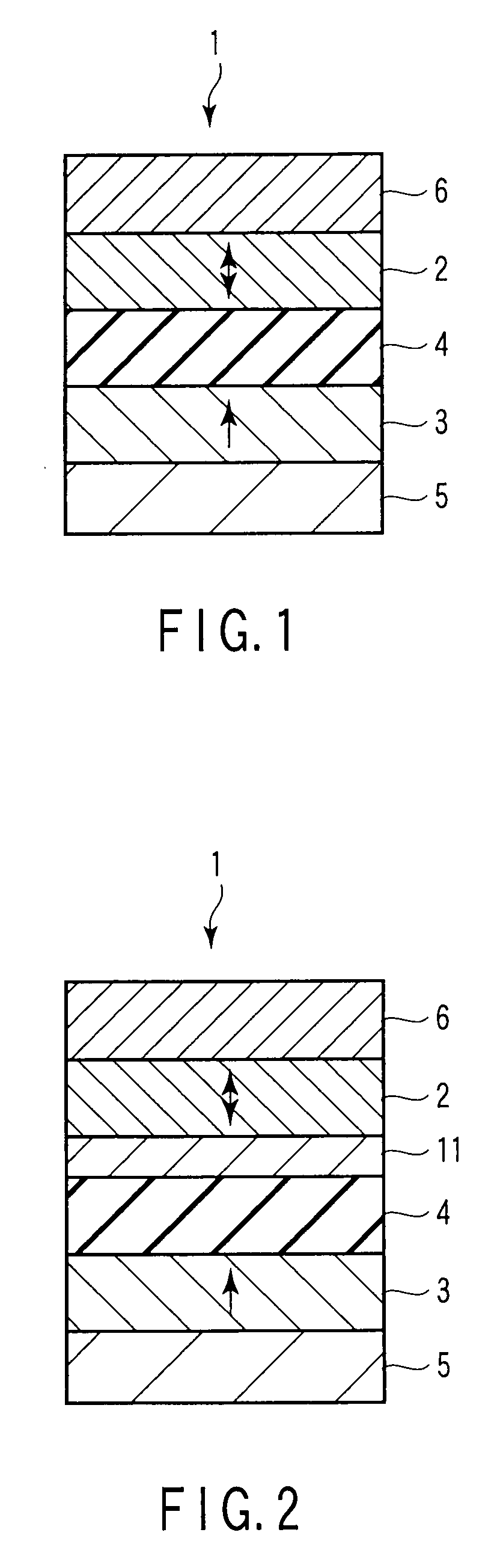
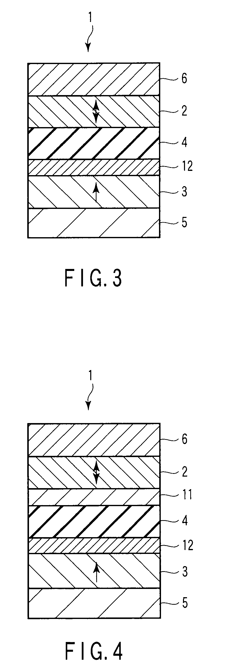
[0031]FIG. 1 shows the main parts of the MR element according to the first embodiment of the present invention. FIG. 1 shows an MR element having a so-called single pin structure. Referring to FIG. 1, arrows indicate the magnetization directions. The MR element herein mentioned in this specification and in the scope of claims is a general term of a GMR (Giant MagnetoResistance) element using a metal spacer layer, and a TMR (Tunneling MagnetoResistance) element using a semiconductor or insulator as a spacer layer. Although the following figures each illustrate the major components of the MR element, another layer may also be included as long as the arrangement shown in the figure is included.

[0032]An MR element 1 has an arrangement in which each layer takes one of two steady states in accordance with the direction of an electric current flowing through surfaces (film surfaces) through which individual ...

second embodiment

[0125]The second embodiment is directed to an MRAM using the MR element of the present invention.

[0126]A spin transfer torque writing type MRAM will be explained below.

[0127]FIG. 12 is a sectional view showing the main parts of a memory cell of the MRAM according to the second embodiment of the present invention. As shown in FIG. 12, the upper surface of an MR element 1 is connected to a bit line 32 via an upper electrode 31. The lower surface of the MR element 1 is connected to a source / drain diffusion region 37a on the surface of a semiconductor substrate 36 via a lower electrode 33, conductive layer (extracting line) 34, and plug 35.

[0128]The source / drain diffusion region 37a forms a selection transistor Tr together with a source / drain diffusion region 37b, a gate insulating film 38 formed on the substrate 36, and a gate electrode 39 formed on the gate insulating film 38. The selection transistor Tr and MR element 1 form a memory cell of the MRAM.

[0129]The source / drain diffusion ...


PUM


Abstract

A magnetoresistive effect element includes a first magnetic layer, a second magnetic layer, and a first spacer layer. The first magnetic layer has an invariable magnetization direction. The second magnetic layer has a variable magnetization direction, and contains at least one element selected from Fe, Co, and Ni, at least one element selected from Ru, Rh, Pd, Ag, Re, Os, Ir, Pt, and Au, and at least one element selected from V, Cr, and Mn. The spacer layer is formed between the first magnetic layer and the second magnetic layer, and made of a nonmagnetic material. A bidirectional electric current flowing through the first magnetic layer, the spacer layer, and the second magnetic layer makes the magnetization direction of the second magnetic layer variable.

Description

CROSS-REFERENCE TO RELATED APPLICATIONS[0001]This application is based upon and claims the benefit of priority from prior Japanese Patent Application No. 2007-094625, filed Mar. 30, 2007, the entire contents of which are incorporated herein by reference.BACKGROUND OF THE INVENTION[0002]1. Field of the Invention[0003]The present invention relates to a magnetoresistive effect element and a magnetoresistive random access memory using the same and, more particularly, to a spin transfer torque writing type magnetoresistive effect element.[0004]2. Description of the Related Art[0005]Recently, many solid-state memories that record information on the basis of new principles have been proposed. Of these solid-state memories, a magnetoresistive random access memory (MRAM) using the tunnel magnetoresistive (TMR) effect is known as a solid-state magnetic memory. The MRAM uses a magnetoresistive effect element (TMR element) that achieves the tunneling magnetoresistive effect as a memory cell, an...

Claims


Application Information

Patent Timeline
Patent Type & Authority Applications(United States)
IPC IPC(8): G11C11/00H01L29/82
CPCG11C11/16H01L27/228H01L43/10Y10S977/935G11C11/161H10B61/22H10N50/85G11B5/39G11C11/15
Inventor YOSHIKAWA, MASATOSHIKITAGAWA, EIJIKAI, TADASHINAGASE, TOSHIHIKOKISHI, TATSUYAYODA, HIROAKI
Owner KIOXIA CORP
Why Eureka
Try Eureka