Process cartridge and image forming apparatus using same

a technology of image forming apparatus and process cartridge, which is applied in the direction of electrographic process, instruments, corona discharge, etc., can solve the problems of reducing the useful life of the photoconductor, abrasion of the rubber blade and the surface layer of the photoconductor, and short life of the cleaning blad

Inactive Publication Date: 2008-10-16
RICOH KK
View PDF6 Cites 17 Cited by
  • Summary
  • Abstract
  • Description
  • Claims
  • Application Information

AI Technical Summary

Benefits of technology

[0017]In view of the aforementioned background, the present disclosure discloses a process cartridge and an image forming apparatus having a photoconductor effectively coated with a protective agent.
[0018]In an aspect of the present disclosure, a process cartridge includes a protective agent, a photoconductor, a charging unit, a development unit, a cleaning unit, and an application unit. The protective agent includes paraffin as a main component. The photoconductor has a surface including polycarbonate to be applied with the protective agent, to which a latent image is to be formed. The charging unit uniformly charges the photoconductor. The development unit develops the latent image formed on the photoconductor as a toner image using a developing agent including toner particles. The cleaning unit removes toner particles remaining on the surface of the photoconductor after the toner image is transferred to a transfer member. The application unit applies the protective agent to the surface of photoconductor. A C1s spectrum of the photoconductor, detected by X-ray photoelectron spectroscopy (XPS) analysis before and after applying the protective agent on the photoconductor, includes a plurality of peaks, corresponding to different carbon binding energy. One of the plurality of peaks in a binding energy range of 290.3 eV to 294 eV is used as target peak to determine a coating condition of the photoconductor coated by the protective agent. A peak area of the target peak with respect to a total area of C1s spectrum of the photoconductor is detected before and after applying the protective agent as a first peak area ratio A0 (%) and a second peak area ratio A (%) to determine a coating condition of the photoconductor, respectively. The first peak area ratio A0 (%) is detected as a value before applying the protective agent, and the photoconductor having the first peak area ratio A0 (%) of 3% or more is employed. The second peak area ratio A (%) is detected as a value after applying the protective agent. The photoconductor is applied with the protective having a coating ratio of 60% or more, computed by (A0−A) / A0×100(%).
[0019]In another aspect of the present disclosure, an image forming apparatus includes a process cartridge. The process cartridge includes a protective agent, a photoconductor, a charging unit, a development unit, a cleaning unit, and an application unit. The protective agent includes paraffin as a main component. The photoconductor has a surface including polycarbonate to be applied with the protective agent, to which a latent image is to be formed. The charging unit uniformly charges the photoconductor. The development unit develops the latent image formed on the photoconductor as a toner image using a developing agent including toner particles. The cleaning unit removes toner particles remaining on the surface of the photoconductor after the toner image is transferred to a transfer member. The application unit applies the protective agent to the surface of photoconductor. A C1s spectrum of the photoconductor, detected by X-ray photoelectron spectroscopy (XPS) analysis before and after applying the protective agent on the photoconductor, includes a plurality of peaks, corresponding to different carbon binding energy. One of the plurality of peaks in a binding energy range of 290.3 eV to 294 eV is used as target peak to determine a coating condition of the photoconductor coated by the protective agent. A peak area of the target peak with respect to a total area of C1s spectrum of the photoconductor is detected before and after applying the protective agent as a first peak area ratio A0 (%) and a second peak area ratio A (%) to determine a coating condition of the photoconductor, respectively. The first peak area ratio A0 (%) is detected as a value before applying the protective agent, and the photoconductor having the first peak area ratio A0 (%) of 3% or more is employed. The second peak area ratio A (%) is detected as a value after applying the protective agent. The photoconductor is applied with the protective having a coating ratio of 60% or more, computed by (A0−A) / A0×100(%).
[0020]In another aspect of the present disclosure, a method of detecting a surface condition of a photoconductor for use in an image forming apparatus is employed when the photoconductor is coated with a protective agent having paraffin as a main component when used in the image forming apparatus. The method includes a) measuring, b) determining, c) determining, and d) computing. In a) measuring, a C1s spectrum of the photoconductor having polycarbonate is measured. In b) determining, a surface condition of the photoconductor before being applied with the protective agent is detected using a target range of binding energy of the photoconductor in the C1s spectrum. The surface condition of the photoconductor before being applied with the protective agent is determined as a first peak area ratio A0 (%) with respect to a total peak area of the C1s spectrum. The photoconductor having the first peak area ratio A0 (%) of 3% or more is employed and the target range of binding energy corresponds to a binding energy of the polycarbonate. In c) determining, a surface condition of the photoconductor after being applied with the protective agent is detected using the target range of binding energy of the photoconductor in the C1s spectrum as a second peak area ratio A (%) with respect to a total peak area of the C1s spectrum. In d) computing, a coating ratio of the photoconductor coated by the protective agent is computed as (A0−A) / A0×100(%).

Problems solved by technology

However, such cleaning blade has a short lifetime and itself reduces the useful life of the photoconductor because the cleaning blade is pressed against the photoconductor to remove residual materials remaining on the photoconductor.
More specifically, frictional pressure between the cleaning blade and the photoconductor causes abrasion on the rubber blade and a surface layer of a photoconductor.
Further, small-sized toner particles, used for coping with demand for higher quality images, may not be effectively trapped by such a cleaning blade, referred to as “passing of toner” or “toner passing.” Such toner passing is more likely to occur by insufficient dimensional or assembly precision of the cleaning blade or when the cleaning blade vibrates unfavorably due to an external shock or the like.
If such toner passing occurs, higher quality images may not be produced.
However, zinc stearate may adhere to a charge roller of an image forming apparatus and cause unfavorable charging condition, which may result in a lower quality image, for example an image having black streaks.
However, paraffin requires more time to coat the surface of photoconductor compared to zinc stearate after application, by which the photoconductor has some areas coated with paraffin and other areas not coated with paraffin.
Such uneven coating may occur when an image forming apparatus, newly shipped from a factory, is used for an image forming operation for the first time.
However, when a protective agent, such as paraffin, not containing metal component is applied to the OPC, XPS analysis shows only peak values for carbon (C) and oxygen (O), and therefore the amount of protective agent applied to the photoconductor may not be correctly evaluated.
If the amount of protective agent on a photoconductor cannot be correctly evaluated, a photoconductor having an insufficient amount of protective agent may be assembled in a process cartridge or an image forming apparatus, and such photoconductor can cause image quality degradation.
As such, a conventional analysis method may not be suitable for detecting an amount of a protective agent, such as paraffin, not including metal component.

Method used


Image

  • Process cartridge and image forming apparatus using same
  • Process cartridge and image forming apparatus using same
  • Process cartridge and image forming apparatus using same

Examples


experiment 1

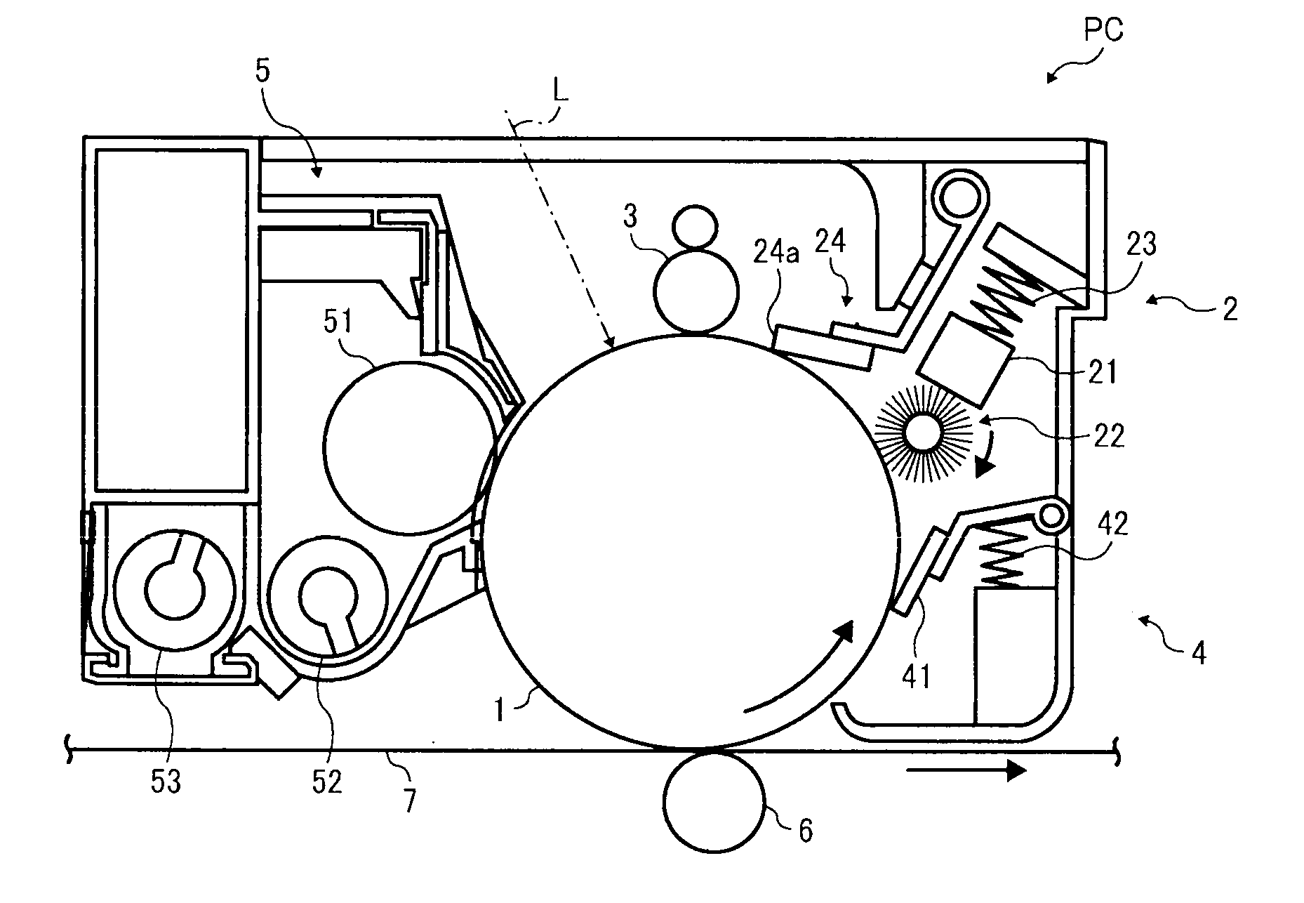
[0265]The photoconductor drum, a brush roller (polyester single fiber having a diameter of 33 μm, fiber density of 50,000 fibers per square inch, prepared by electrostatic implantation method), and a urethane blade were assembled in a protective agent setting unit and a process cartridge. The protective agent bar No. 2 was pressed to the brush with a spring force of 4.8 N to apply a protective agent to the photoconductor drum for 40 minutes. The photoconductor drum and the brush roller rotated at a linear velocity of 125 mm / sec and 146 mm / sec, respectively. In such preparation process, a developing unit and a charge roller were removed from the process cartridge.

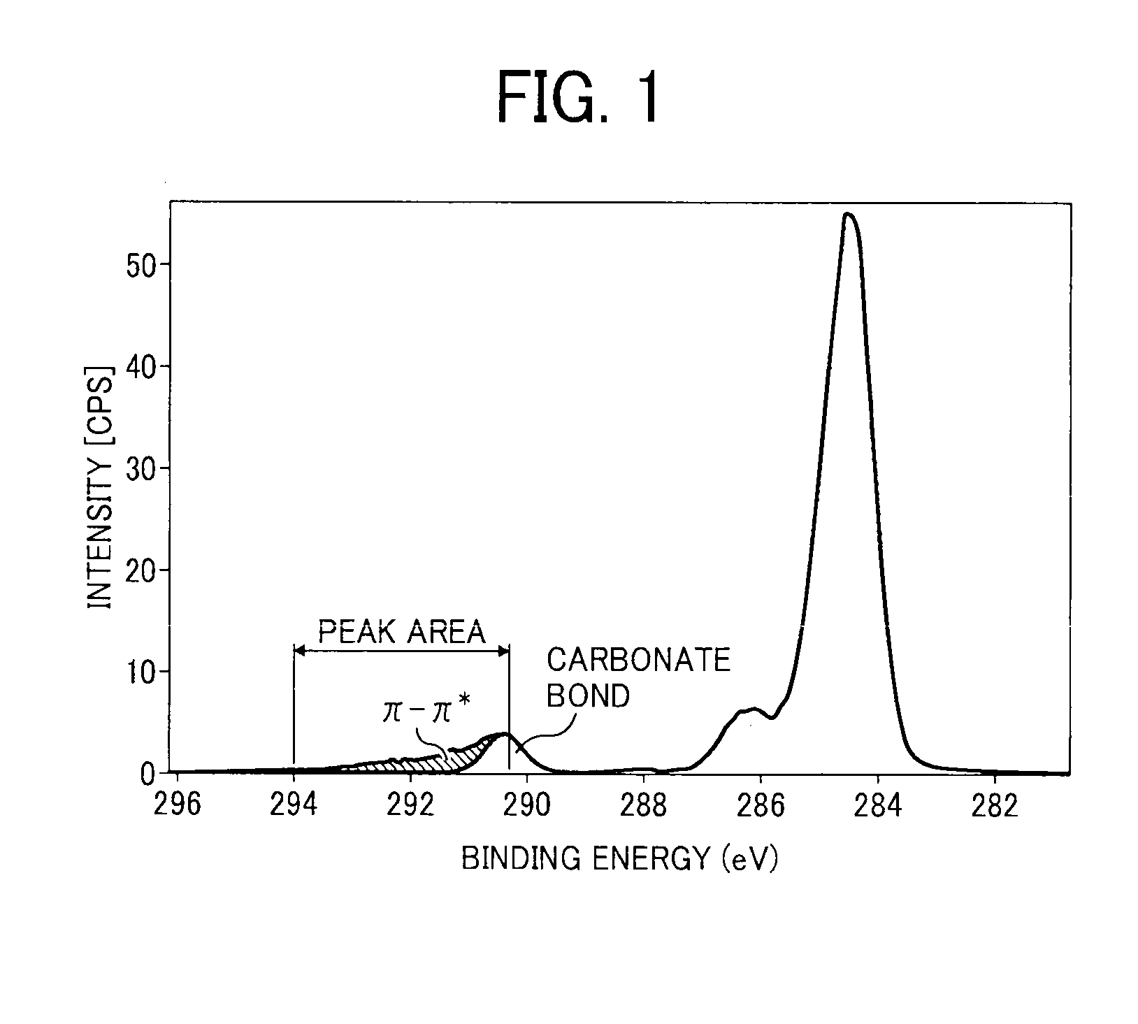
[0266]The second area value A of the photoconductor drum after applying the protective agent was detected as 0% by using an XPS analysis. Accordingly, a coating ratio of the photoconductor drum, defined by ((A0−A) / A0×100)(%), was measured as 100%.

[0267]As above described, the A and A0 are a ratio of peak area of 290.3 eV to ...

experiment 2

[0271]Except a brush roller (polyester single fiber having a diameter of 39 μm, fiber density of 50,000 fibers per square inch, prepared by electrostatic implantation method), same devices used in Experiment 1 were used, and the protective agent was applied to the photoconductor drum for 40 minutes.

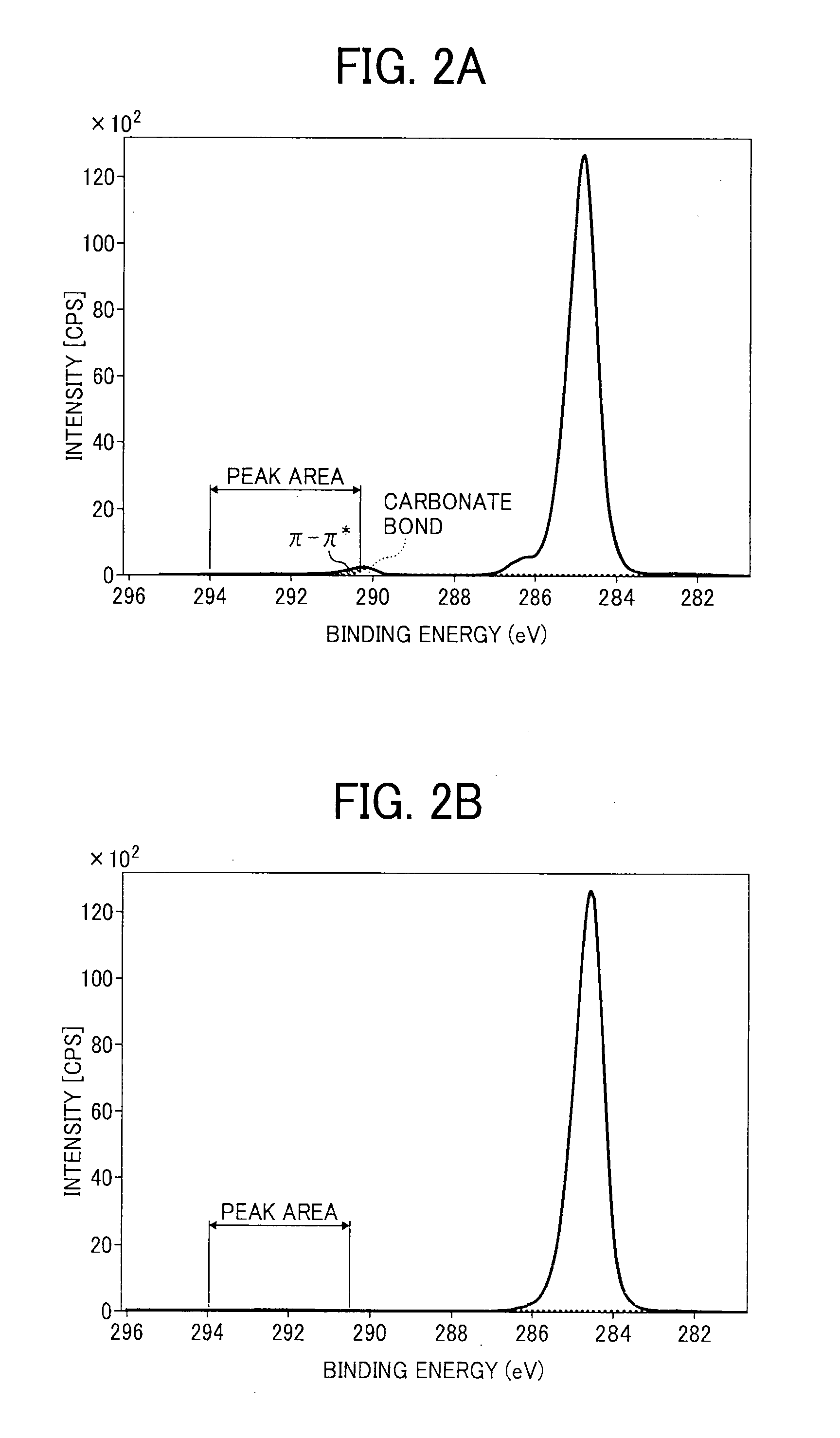
[0272]The second area value A of the photoconductor drum after applying the protective agent was detected as 0% using an XPS analysis. Accordingly, a coating ratio of the photoconductor drum, defined by ((A0−A) / A0×100)(%), was measured as 100%.

[0273]When evaluating performance of an image forming apparatus, a new photoconductor drum was assembled in a process cartridge as the photoconductor drum, and the protective agent was applied to the photoconductor drum for 40 minutes. Then, a developing unit and a charge roller were set in the process cartridge. The process cartridge was installed in IPSIO CX400, a tandem type color image forming apparatus produced by Ricoh Company, Ltd. In the pro...

experiment 3

[0275]Except a brush roller (polyester single fiber having a diameter of 39 μm, fiber density of 30,000 fibers per square inch, prepared by electrostatic implantation method) and pressing the protective agent bar No. 1 with a spring force of 2N, same devices used in Experiment 1 were used, and a protective agent was applied to the photoconductor drum for 40 minutes.

[0276]The second area value A of the photoconductor drum after applying protective agent was detected as 4.8% using an XPS analysis. Accordingly, a coating ratio of the photoconductor drum, defined by ((A0−A) / A0×100)(%), was measured as 45%, in which the first area value A0 was 8.7% as above described.

[0277]When evaluating performance of an image forming apparatus, a new photoconductor drum was assembled in a process cartridge as the photoconductor drum, and the protective agent was applied to the photoconductor drum for 40 minutes. Then, a developing unit and a charge roller were set in the process cartridge. The process...


PUM

PropertyMeasurementUnit
binding energyaaaaaaaaaa
diameteraaaaaaaaaa
binding energyaaaaaaaaaa

Abstract

A process cartridge includes a protective agent, a photoconductor, a charging unit, a development unit, a cleaning unit, and an application unit. The protective agent includes paraffin as main component. The photoconductor has a surface including polycarbonate applied with the protective agent. The development unit develops a latent image on the photoconductor. The cleaning unit removes materials remaining on the photoconductor. The application unit applies the protective agent to the surface of photoconductor. One peak in a given binding energy range is used to determine a coating condition of the photoconductor coated by the agent. The coating condition is determined by comparing an area ratio A0 before applying the agent and an area ratio A after applying the agent, each of which is an area ratio with respect to a total area of C1s spectrum of the photoconductor. The coating ratio of the photoconductor is computed by (A0−A)/A0×100.

Description

CROSS-REFERENCE TO RELATED APPLICATIONS[0001]This application claims priority from Japanese Patent Application Nos. 2007-106214, filed on Apr. 13, 2007, and 2008-033704, filed on Feb. 14, 2008 in the Japan Patent Office, the entire contents of each of which are hereby incorporated by reference herein.BACKGROUND OF THE INVENTION[0002]1. Field of the Invention[0003]The present disclosure generally relates to a process cartridge used for an image forming apparatus, and more particularly, to a process cartridge having a function of applying a protective agent to a photoconductor.[0004]2. Description of the Background Art[0005]Typically, an image forming apparatus using electrophotography produces an image by sequentially conducting a series of processes such as a charging process, an exposure process, a developing process, and a transfer process to a photoconductor such as an OPC (organic photoconductor). After conducting the transfer process, by-products generated by discharging during...

Claims


Application Information

Patent Timeline
Patent Type & Authority Applications(United States)
IPC IPC(8): G03G21/18
CPCG03G5/043G03G5/14721G03G5/14756G03G15/751G03G21/1828G03G2221/1609
Inventor HATAKEYAMA, KUMIKOKABATA, TOSHIYUKIYAMASHITA, MASAHIDE
Owner RICOH KK
Why Eureka
Try Eureka