Multi-band burst-mode clock and data recovery circuit

a multi-band burst-mode clock and data recovery technology, applied in the direction of pulse generator, pulse technique, electric pulse generator circuit, etc., can solve the problems of significant inter-symbol interference (isi), the half bit-time delay line limits the jitter tolerance and bit-error rate, and the difficulty of the conventional cdr circuit to settle within such a short tim

Active Publication Date: 2008-10-23
MEDIATEK INC +1
View PDF11 Cites 36 Cited by
  • Summary
  • Abstract
  • Description
  • Claims
  • Application Information

AI Technical Summary

Problems solved by technology

It is difficult for the conventional CDR circuits to settle within such a short time.
The accuracy of the half bit-time delay line limits the jitter tolerance and bit-error rate.
The result is significant inter-symbol interference (ISI) caused by random data patterns for the GVCOs.
Moreover, the delay cells in a GVCO are composed of logic gates instead of simple inverters, which increase the bandwidth requirement of the delay cells.

Method used


Image

  • Multi-band burst-mode clock and data recovery circuit
  • Multi-band burst-mode clock and data recovery circuit
  • Multi-band burst-mode clock and data recovery circuit

Examples


Embodiment Construction

[0022]The following description is of the best-contemplated mode of carrying out the invention. This description is made for the purpose of illustrating the general principles of the invention and should not be taken in a limiting sense. The scope of the invention is best determined by reference to the appended claims.

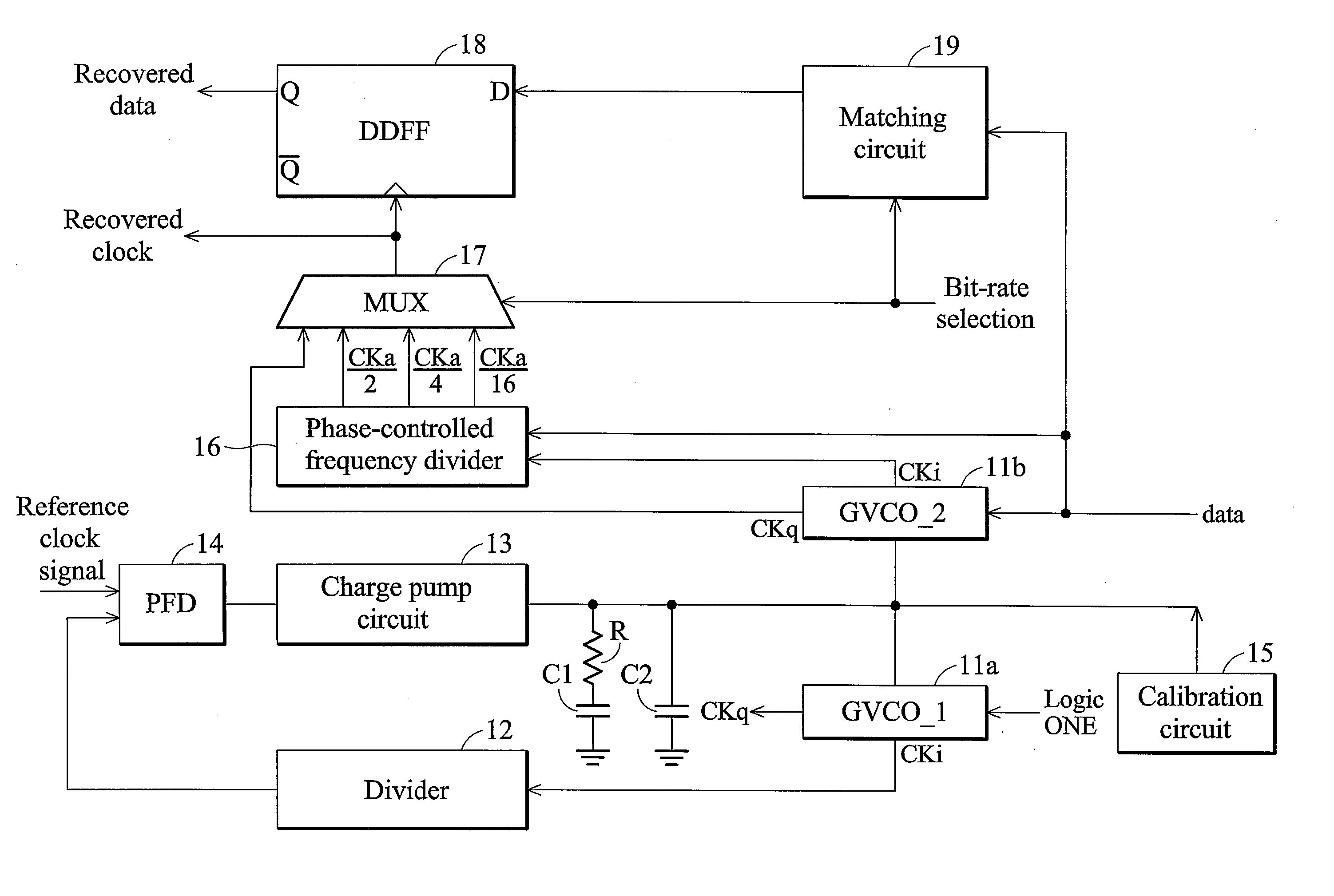
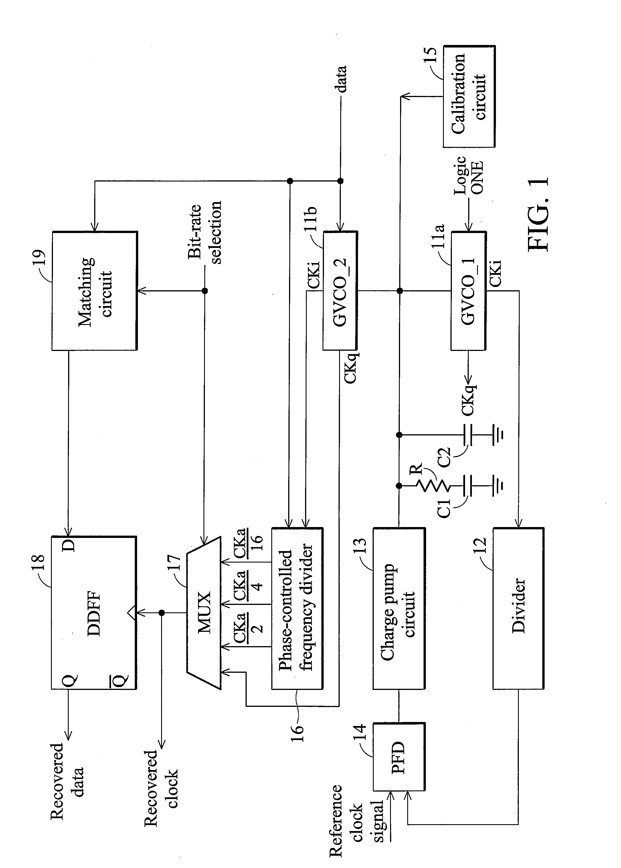
[0023]FIG. 1 is a schematic diagram of an embodiment of a clock and data recovery circuit according to the invention. The clock and data recovery circuit (CDR) comprises a PLL unit composing of the phase frequency detector (PHD) 14, the charge pump circuit 13, the gated voltage-controlled oscillator 11a (GVCO_1), and the divider 12. In the embodiment, the GVCO_111a can be regarded as a replica GVCO of the GVCO_211b. The GVCO_111a is connected to logic ONE and receives the reference voltage Vc to generate the clock signal CKi and CKq, wherein a phase delay exits between the clock signal CKi and CKq. The divider 12 receives and divides the clock signal CKi by a parameter...


PUM


Abstract

A clock and data recovery circuit is disclosed and comprises a first gated voltage-controlled oscillator, a PLL unit, a phase-controlled frequency divider, a multiplexer, a matching circuit and a double-edge-triggered D flip-flop. The first GVCO receives a data signal and a reference voltage to generate a first clock signal and a second clock signal based on the data signal. The PLL unit receives a reference clock signal and generates the reference voltage to adjust the frequency of the first clock signal and the second clock signal at the vicinity of the predetermined frequency. The phase-controlled frequency divider receives and divides the first clock signal by N to output a third clock signal. The multiplexer controlled by a selection signal receives and outputs the second clock signal or the third clock signal. The matching circuit receives the data signal and the selection signal to match the delays therebetween. The double-edge-triggered D flip-flop comprises a data input terminal receiving the output signal from the matching circuit, a clock input terminal receiving the output signal from the multiplexer, and an output terminal outputting a recovered data signal.

Description

CROSS REFERENCE TO RELATED APPLICATIONS[0001]This application claims the benefit of U.S. Provisional Application No. 60 / 912,700, filed Apr. 19, 2007.BACKGROUND OF THE INVENTION[0002]1. Field of the Invention[0003]The invention relates to a clock and data recovery circuit, and more particularly to a multi-band burst-mode clock and data recovery circuit.[0004]2. Description of the Related Art[0005]Passive optical networks (PONs) solve bottlenecks among back-bone networks and LANs. To connect many optical network units (ONUs) with an optical line termination (OLT), the time division multiple access (TDMA) scheme is adopted. Therefore, the OLT may receive the sequent burst-mode data from ONUs. The clock and data recovery (CDR) circuit at the OLT must detect the input data within tens of bit times and recover the clock and data. It is difficult for the conventional CDR circuits to settle within such a short time. Conventional gated voltage-controlled oscillators (GVCOs) are roughly class...

Claims


Application Information

Patent Timeline
Patent Type & Authority Applications(United States)
IPC IPC(8): H04L7/00H03L7/099
CPCH03L7/0805H03L7/099H03L7/0995H03L7/18H04L7/033
Inventor LIANG, CHE-FUHWU, SY-CHYUAN
Owner MEDIATEK INC
Why Eureka
Try Eureka