Organic light emitting device

a light-emitting device and organic technology, applied in semiconductor devices, instruments, computing, etc., can solve the problems of easy deformation, easy deformation of the emitting layer, and hardly providing a uniform screen image quality, so as to prevent interference between lines and uniform image quality

Active Publication Date: 2008-10-30
LG DISPLAY CO LTD
View PDF2 Cites 17 Cited by
  • Summary
  • Abstract
  • Description
  • Claims
  • Application Information

AI Technical Summary

Benefits of technology

[0014]Exemplary embodiments provide an organic light emitting device capable of providing uniform image quality by preventing interference between lines.

Problems solved by technology

Because the organic light emitting device includes the emitting layer including the organic material, it is easily degraded when external moisture or oxygen is infiltrated into the display device.
Also, as a driving time of the organic light emitting device is lengthened, the emitting layer is readily degraded by heat generated in a driving unit.
Thus, because the amount of voltage to be applied to obtain the same luminance varies according to a degradation degree or according to the surroundings, the organic light emitting device has disadvantages in that it can hardly provide a uniform quality of screen images.
However, measurement of voltage of the monitor pixels is performed while the organic light emitting device is being driven, so a problem arises in that there is a deviation in each size of measured voltages.
In other words, because the signal applied to the monitor pixels is DC power and a data signal applied to the subpixels is an alternating current (AC) signal, a signal interference is caused between lines transferring the DC power to the monitor pixels and lines transferring the data signal to the subpixels positioned to be adjacent to the monitor pixels, resulting in that the size of the measured voltage may be different.
Thus, it is difficult to provide an accurate compensation voltage in consideration of the degradation of the subpixels of the display unit and temperature.

Method used


Image

  • Organic light emitting device
  • Organic light emitting device
  • Organic light emitting device

Examples


Embodiment Construction

[0035]Reference will now be made in detail embodiments of the invention examples of which are illustrated in the accompanying drawings.

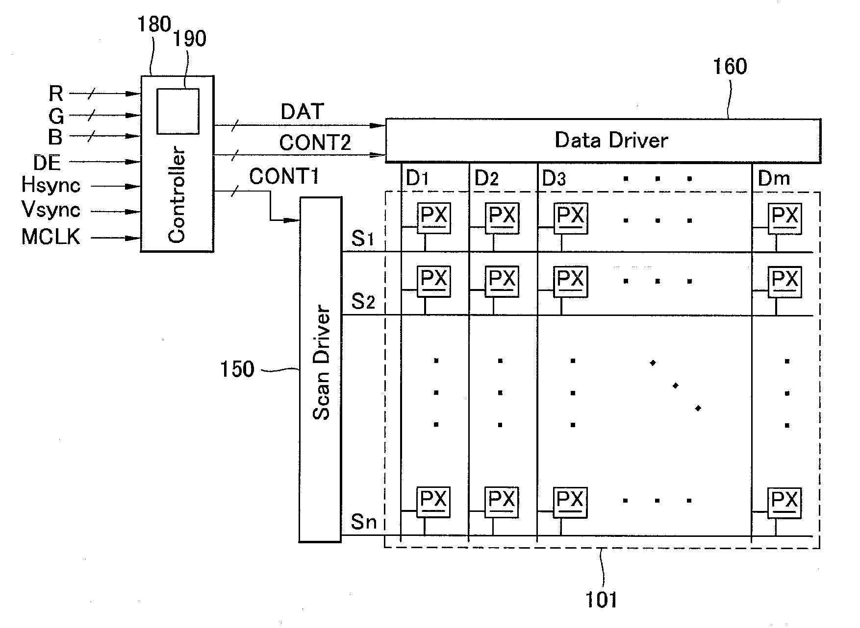
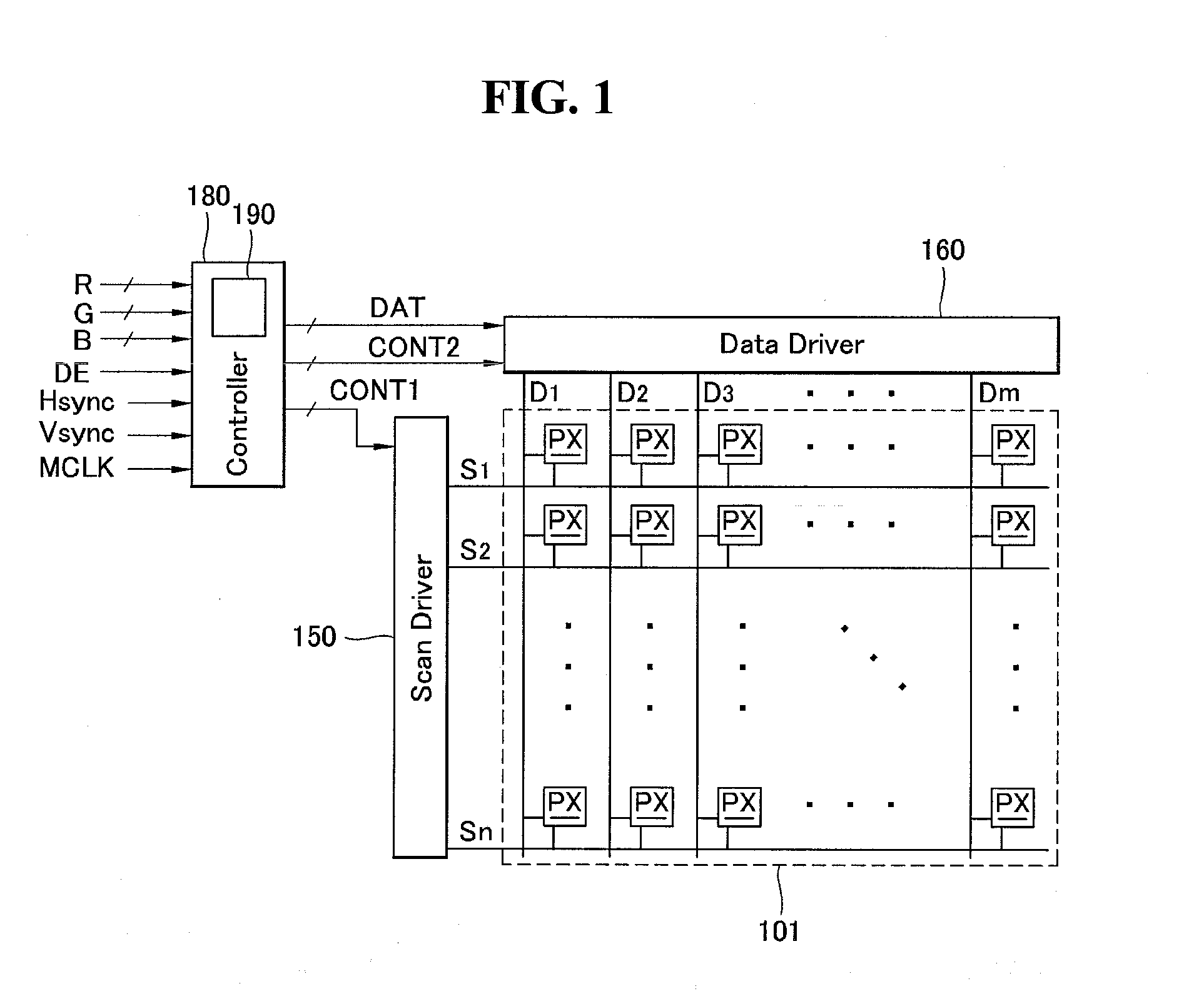
[0036]FIG. 1 is a bock diagram of an organic light emitting device according to an exemplary embodiment.

[0037]As shown in FIG. 1, the organic light emitting device according to the exemplary embodiment includes a display panel 101, a scan driver 150, a data driver 160, and a controller 180.

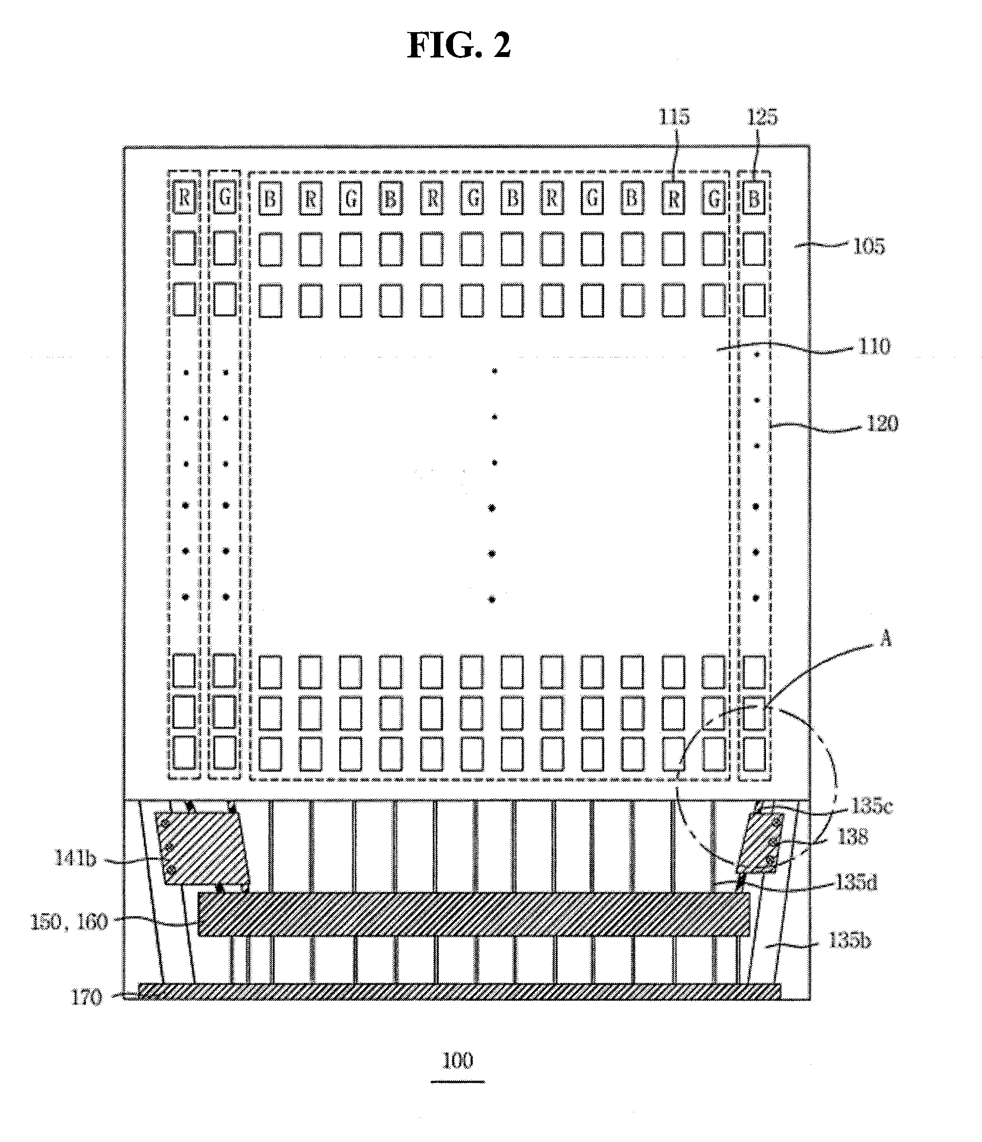
[0038]The display panel 101 includes a plurality of signal lines S1 to Sn and D1 to Dm, a plurality of power supply lines (not shown), and a plurality of subpixels PX connected to the signal lines S1 to Sn and D1 to Dm and the power supply lines in a matrix form. The display panel 101 may further include monitor pixels.

[0039]The plurality of signal lines S1 to Sn and D1 to Dm may include the plurality of scan lines S1 to Sn for sending scan signals and the plurality of data lines D1 to Dm for sending data signals. Each power supply line may send voltages such as a ...


PUM


Abstract

An organic light emitting device is disclosed. The organic light emitting device includes a substrate, a display unit that is positioned on the substrate and includes a subpixel and a monitor pixel, a first line supplying a voltage to the subpixel and the monitor pixel, a second line supplying a direct current (DC) power to the monitor pixel, a third line that transfers an electrical signal used to display an image on the subpixel, and a shield layer that is positioned on or under the second line and is electrically connected to the first line.

Description

[0001]This application claims the benefit of Korean Patent Application No. 10-2007-0041629 filed on Apr. 27, 2007 and No. 10-2007-0047420 filed on May 16, 2007, which is hereby incorporated by reference.BACKGROUND OF THE DISCLOSURE[0002]1. Field of the Disclosure[0003]Exemplary embodiments relate to a display device and, more particularly, to an organic light emitting device.[0004]2. Description of the Related Art[0005]Out of flat panel display devices, a light emitting device is a self-emission display device that does not require a backlight unit and has such characteristics that it can be fabricated to be light and thin, its process can be simplified. Further, the light emitting device can be fabricated at a low temperature, has a high response speed of 1 ms or lower, low power consumption, a wide viewing angle, and high contrast ratio, etc.[0006]In particular, an organic light emitting device includes an emitting layer including an organic material between an anode electrode and...

Claims


Application Information

Patent Timeline
Patent Type & Authority Applications(United States)
IPC IPC(8): G06F3/038G09G3/12
CPCG09G3/2018G09G3/3225G09G2300/0426G09G2360/148H01L27/3223H01L27/326H01L27/3272H01L27/3276H10K59/88H10K59/121H10K59/126H10K59/131
Inventor KIM, SEUNGTAE
Owner LG DISPLAY CO LTD
Why Eureka
Try Eureka