Method of forming thin film solar cells

a solar cell and film technology, applied in the field of thin film solar cell forming, can solve the problems of limited throughput of substrates and substantial slowdown of production, and achieve the effects of improving collection efficiency, high collection efficiency, and high collection efficiency

Inactive Publication Date: 2008-11-06
APPLIED MATERIALS INC
View PDF12 Cites 48 Cited by
  • Summary
  • Abstract
  • Description
  • Claims
  • Application Information

AI Technical Summary

Benefits of technology

[0020]It is possible to use a single chamber process to form thin film p-i-n solar cells and still achieve collection efficiencies in the range of 9% to 9.5%, and expectedly higher as development continues. These relatively high collection efficiencies (compared with previous collection efficiencies for thin film solar cells) can be achieved using a single chamber manufacturing process by: 1) altering the overall chemical and structural composition of the p-doped and/or n-doped silicon-containing layer from that previously known art, to provide a silicon-carbide containing composition and structure within the p-doped layer, whereby the collection ef

Problems solved by technology

In the “three” chamber process, substrate throughput is limited by the need to transfer substrates between processing chambers.
Even if there were

Method used


Image

  • Method of forming thin film solar cells
  • Method of forming thin film solar cells
  • Method of forming thin film solar cells

Examples


example one

Formation of a Single Junction Solar Cell

[0076]FIG. 3 shows a single stack (single junction) thin film solar cell, which includes a glass substrate 302, top electrode 304, p-layer 306, i-layer 308, n-layer 310, bottom electrode 312, and reflector 314. The interface between p-doped layer 306 and i-layer 308 is illustrated as 307.

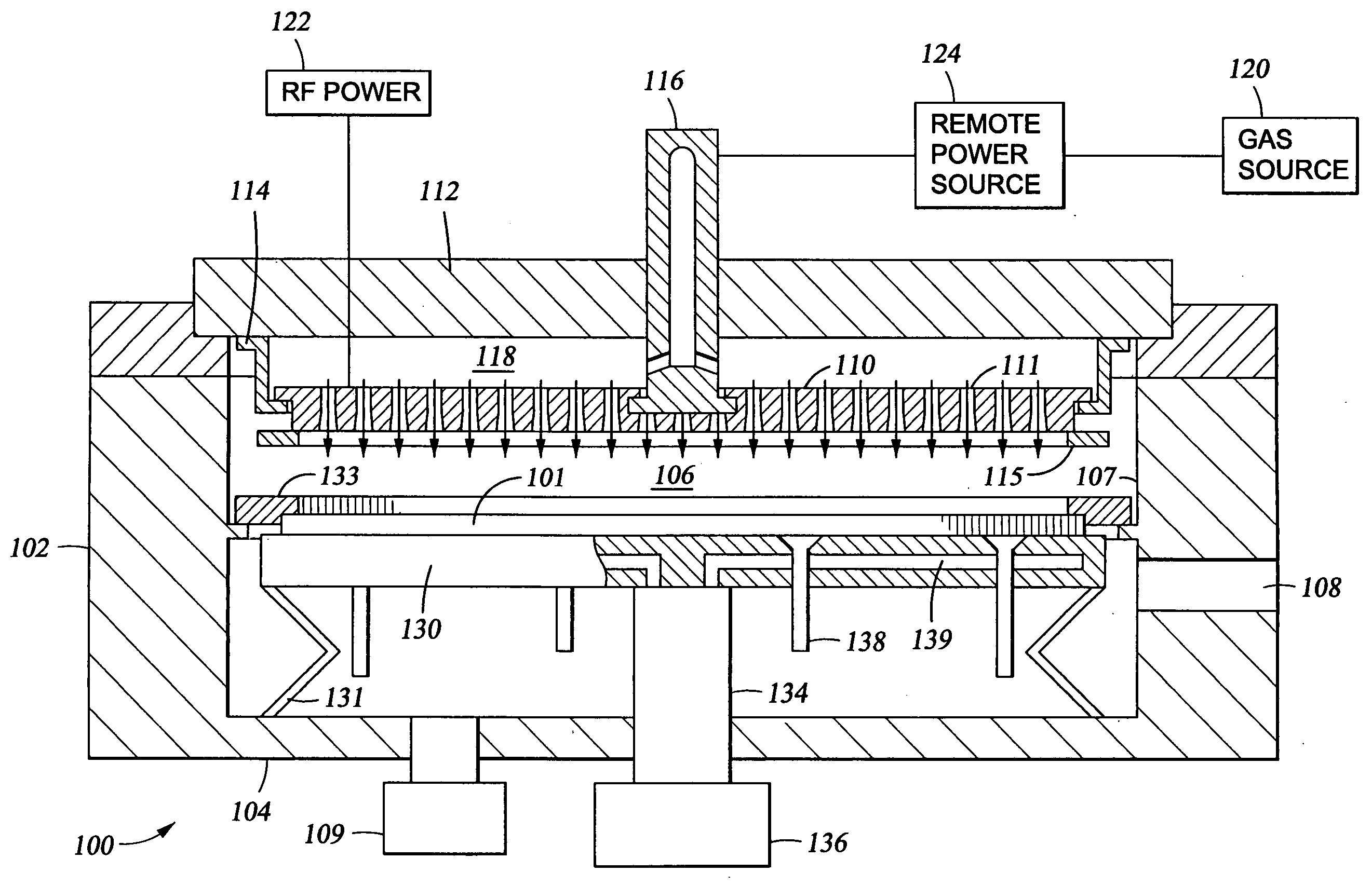
[0077]The process steps described herein are those required for deposition of the thin film silicon-containing layers of the kind previously described, where the layers are deposited using PECVD. When all of the silicon-comprising layers in the solar cell are a-silicon-comprising layers (as they are for the single junction solar cell shown in FIG. 3), the PECVD depositions may be made using one of the single processing chambers 230 in cluster processing tool 203, of the kind shown in FIG. 2C. Each of the P / I / N processing chambers 230 for depositing silicon-comprising layers are essentially the same, and are capable of depositing a-silicon. It is also possible...

example two

Formation of a Dual / Tandem Junction Solar Cell

[0085]FIG. 4 shows a dual stack (dual junction) thin film solar cell, which includes a glass substrate 402; top electrode 404; a top p-i-n cell including: a p-doped layer comprising a-silicon 406; i-layer comprising a-silicon 408; and a dual n-doped layer, including a first n-doped layer comprising a-silicon 410, and a second n-doped layer comprising mc-silicon 412; a bottom p-i-n cell including: a p-doped layer comprising mc-silicon 414; i-layer comprising mc-silicon 416; n-doped layer comprising a-silicon 418; a bottom electrode of ZnO TCO 420, and an aluminum or silver reflector 422. An example interface between p-doped layer 406 and i-layer 408 is designated as 407.

[0086]The process steps described herein are limited to the steps required for deposition of the thin film silicon-containing layers previously described, where the layers are deposited using PECVD. The PECVD depositions are made using a cluster processing system 240 of th...

example three

Formation of an Alternative Dual / Tandem Junction Solar Cell

[0099]FIG. 5 shows an alternative dual stack (dual junction) thin film solar cell, which includes a glass substrate 502; top electrode 504; a top p-i-n cell including: a dual p-doped layer comprising an upper portion of mc-silicon 505 and a lower portion of a-silicon 506; i-layer comprising a-silicon 508; and a dual n-doped layer, including a first n-doped layer comprising a-silicon 510, and a second n-doped layer comprising mc-silicon 512; a bottom p-i-n cell including: a p-doped layer comprising mc-silicon 514; i-layer comprising mc-silicon 516; n-doped layer comprising a-silicon 518; a bottom electrode of ZnO TCO 520, and an aluminum or silver reflector 522.

[0100]The process steps described herein are limited to the steps required for deposition of the thin film silicon-containing layers previously described, where the layers are deposited using PECVD. The PECVD depositions are made using a cluster processing system 240 o...


PUM

PropertyMeasurementUnit
Temperatureaaaaaaaaaa
Areaaaaaaaaaaa

Abstract

A single chamber CVD manufacturing process enables thin film p-i-n solar cells exhibiting collection efficiencies in the range of 9% to 12%, and higher. These collection efficiencies are achieved by: Changing the overall chemical and structural composition of the p-doped layer; Using techniques to remove residual reactants after deposition of the p-doped layer; optionally, applying a buffer layer of a hydrogen-rich amorphous silicon between the p-doped layer and a subsequently deposited intrinsic layer; and, changing the silicon crystalline composition during deposition of an i-doped layer or an n-doped layer. The single chamber process provides a cost of manufacture/solar cell output in $/Watt that is competitive.

Description

BACKGROUND OF THE INVENTION[0001]1. Field of the Invention[0002]The present invention pertains to a method of forming thin film solar cells. In addition, the present invention pertains to a method of reducing the p-dopant contamination at an interface of a p-doped layer and an intrinsic layer of a thin film solar cell.[0003]2. Brief Description of the Background Art[0004]This section describes background subject matter related to the disclosed embodiments of the present invention. There is no intention, either express or implied, that the background art discussed in this section legally constitutes prior art.[0005]Solar cell technology, a desirable clean energy source, remains too costly when compared with conventional energy sources, thus preventing the widespread use of solar power. Therefore it is desirable to reduce the cost of the manufacture and improve the performance of solar cells. The commonly used methods of solar cell manufacture make use of crystalline silicon, which ac...

Claims


Application Information

Patent Timeline
IPC IPC(8): H01L31/18C23C16/00
CPCC23C16/24C23C16/54H01L31/076H01L31/182H01L31/1824Y02E10/545Y02E10/546Y02E10/548Y02P70/50
Inventor CHOI, SOO YOUNGLI, LIWEI
Owner APPLIED MATERIALS INC
Why Eureka
Try Eureka